Service Manuals, User Guides, Schematic Diagrams or docs for : . Electronic Components Datasheets Active components Transistors Supertex 2n6660_2n6661
<< Back | HomeMost service manuals and schematics are PDF files, so You will need Adobre Acrobat Reader to view : Acrobat Download Some of the files are DjVu format. Readers and resources available here : DjVu Resources
For the compressed files, most common are zip and rar. Please, extract files with Your favorite compression software ( WinZip, WinRAR ... ) before viewing. If a document has multiple parts, You should download all, before extracting.
Good luck. Repair on Your own risk. Make sure You know what You are doing.
Image preview - the first page of the document
>> Download 2n6660_2n6661 documenatation <<
Text preview - extract from the document
2N6660
2N6661
N-Channel Enhancement-Mode
Vertical DMOS FETs
Ordering Information
Order Number / Package
BVDSS / RDS(ON) ID(ON)
BVDGS (max) (min) TO-39
60V 3.0 1.5A 2N6660
90V 4.0 1.5A 2N6661
High Reliability Devices Advanced DMOS Technology
See pages 5-4 and 5-5 for MILITARY STANDARD Process
These enhancement-mode (normally-off) transistors utilize a
Flows and Ordering Information.
vertical DMOS structure and Supertex's well-proven silicon-gate
manufacturing process. This combination produces devices with
Features the power handling capabilities of bipolar transistors and with the
high input impedance and positive temperature coefficient inher-
s Free from secondary breakdown ent in MOS devices. Characteristic of all MOS structures, these
devices are free from thermal runaway and thermally-induced
s Low power drive requirement
secondary breakdown.
s Ease of paralleling Supertex's vertical DMOS FETs are ideally suited to a wide range
s Low CISS and fast switching speeds of switching and amplifying applications where high breakdown
voltage, high input impedance, low input capacitance, and fast
s Excellent thermal stability
switching speeds are desired.
s Integral Source-Drain diode
s High input impedance and high gain
s Complementary N- and P-channel devices
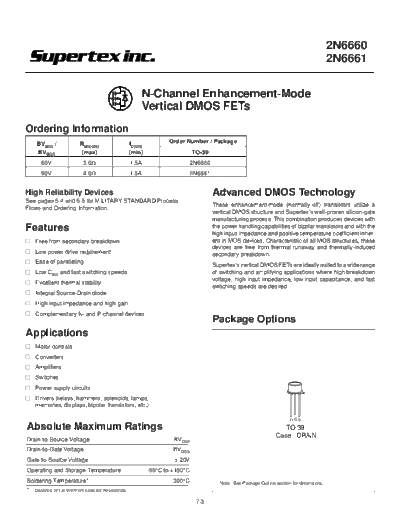
Package Options
Applications
s Motor controls
s Converters
s Amplifiers
s Switches
s Power supply circuits
s Drivers (relays, hammers, solenoids, lamps,
memories, displays, bipolar transistors, etc.)
DGS
Absolute Maximum Ratings TO-39
Case: DRAIN
Drain-to-Source Voltage BVDSS
Drain-to-Gate Voltage BVDGS
Gate-to-Source Voltage ◦ Jabse Service Manual Search 2024 ◦ Jabse Pravopis ◦ onTap.bg ◦ Other service manual resources online : Fixya ◦ eServiceinfo