Service Manuals, User Guides, Schematic Diagrams or docs for : . Electronic Components Datasheets Active components Transistors Rohm dta113tka
<< Back | HomeMost service manuals and schematics are PDF files, so You will need Adobre Acrobat Reader to view : Acrobat Download Some of the files are DjVu format. Readers and resources available here : DjVu Resources
For the compressed files, most common are zip and rar. Please, extract files with Your favorite compression software ( WinZip, WinRAR ... ) before viewing. If a document has multiple parts, You should download all, before extracting.
Good luck. Repair on Your own risk. Make sure You know what You are doing.
Image preview - the first page of the document
>> Download dta113tka documenatation <<
Text preview - extract from the document
DTA113TKA
Transistors
-100mA / -50V Digital transistor
(with built-in resistor)
DTA113TKA
Applications External dimensions (Unit : mm)
Inverter, Interface, Driver
SMT3 2.9 1.1
0.4 0.8
Features
1) Built-in bias resistors enable the configuration of an (3)
inverter circuit without connecting external input
2.8
1.6
resistors.
(2) (1)
2) The bias resistors consist of thin-film resistors with
0.3Min.
0.95 0.95
complete isolation to allow positive biasing of the input, 0.15
(1)Emitter 1.9
and parasitic effects are almost completely eliminated. (2)Base
3) Only the on/ off conditions need to be set for operation, (3)Collector Each lead has same dimension
Abbreviated symbol : 91
making the device design easy.
4) Higher mounting densities can be achieved.
Structure Equivalent circuit
PNP epitaxial planar silicon transistor
(Resistor built-in type)
C
B
R1
Packaging specifications E
Package SMT3 E : Emitter
Packaging type Taping C : Collector
B : Base
Code T146
Part No. Basic ordering unit (pieces) 3000
R1=1k
DTA113TKA
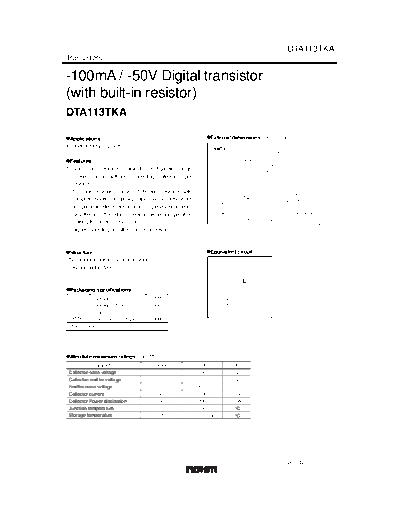
Absolute maximum ratings (Ta=25◦ Jabse Service Manual Search 2024 ◦ Jabse Pravopis ◦ onTap.bg ◦ Other service manual resources online : Fixya ◦ eServiceinfo