Service Manuals, User Guides, Schematic Diagrams or docs for : . Electronic Components Datasheets Active components Transistors Wietron 2n4403

<< Back | Home

Most service manuals and schematics are PDF files, so You will need Adobre Acrobat Reader to view : Acrobat Download Some of the files are DjVu format. Readers and resources available here : DjVu Resources
For the compressed files, most common are zip and rar. Please, extract files with Your favorite compression software ( WinZip, WinRAR ... ) before viewing. If a document has multiple parts, You should download all, before extracting.
Good luck. Repair on Your own risk. Make sure You know what You are doing.


Image preview - the first page of the document
2n4403


>> Download 2n4403 documenatation <<

Text preview - extract from the document
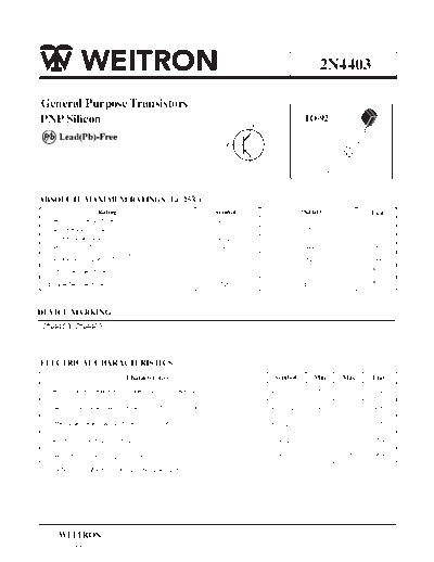
                                                                                                          2N4403

General Purpose Transistors
PNP Silicon                                                               COLLECTOR
                                                                              3
                                                                                                   TO-92

                                                                    2
                                                                  BASE
                                                                                                               1
                                                                                                1. EMITTER         2
                                                                              1                                        3
                                                                                                2. BASE
                                                                          EMITTER
                                                                                                3. COLLECTOR


ABSOLUTE MAXIMUM RATINGS (Ta=25 C)
                    Rating                                       Symbol                           2N4403                   Unit
 Collector-Emitter Voltage                                        VCEO                              -40                     Vdc
 Collector-Base Voltage                                           VCBO                              -40                     Vdc
 Emitter-Base Voltage                                             VEBO                             -5.0                     Vdc
 Collector Current                                                 IC                              -600                    mAdc
 Total Device Dissipation TA=25 C                                  PD                               625                    mW
 Junction Temperature                                              Tj                               150                     C
  Storage Temperature                                             Tstg                          -55 to +150                 C


DEVICE MARKING
 2N4403=2N4403


ELECTRICAL CHARACTERISTICS
                                Characteristics                                        Symbol         Min          Max     Unit
 Collector-Emitter Breakdown Voltage (1) (IC= -1.0 mAdc, IB=0)                        V(BR)CEO         -40             -    Vdc

 Collector-Base Breakdown Voltage (IC= -0.1 mAdc, IE=0)                               V(BR)CBO         -40             -    Vdc

 Emitter-Base Breakdown Voltage (IE= -0.1 mAdc, IC=0)                                 V(BR)EBO         -5.0            -    Vdc

 Base Cutoff Current (VCB= -35 Vdc, IE=0)                                               ICBO              -        -0.1    uAdc

 Collect Cutoff Current(VCE = -35 Vdc, I B =0)                                          I CEO             -        -0.1    uAdc

1. Pulse Test: Pulse Width < 300 us, Duty Cycle < 2.0%


       WEITRON
http://www.weitron.com.tw
            2N4403
ELECTRICAL CHARACTERISTICS (TA=25 C unless otherwise noted) (Countinued)
                               Characteristics                      Symbol     Min     Max     Unit


ON CHARACTERISTICS
 DC Current Gain                                                                                 -
                                                                     hFE                 -
 (IC= -0.1 mAdc, VCE=-1.0 Vdc)                                                  30
 (IC= -1.0 mAdc, VCE=-1.0 Vdc)                                                  60       -
 (IC= -10 mAdc, VCE=-1.0 Vdc)                                                  100       -
 (IC= -150 mAdc, VCE=-2.0 Vdc) (1)                                             100      300
 (IC= -500 mAdc, VCE=-2.0 Vdc) (1)                                              20       -
 Collector-Emitter Saturation Voltage (1)                           VCE(sat)                    Vdc
  (IC= -150 mAdc, IB= -15 mAdc)                                                  -      -0.4
  (IC=- 500 mAdc, IB= -50 mAdc)                                                  -     -0.75

  Base-Emitter Saturation Voltage (1)                               VBE(sat)                    Vdc
   (IC= -150 mAdc, IB= -15 mAdc)                                               -0.75   -0.95
   (IC= -500 mAdc, IB=- 50 mAdc)                                                 -      -1.3


SMALL-SIGNAL CHARACTERISTICS
 Current-Gain-Bandwidth Product                                                                 MHz
                                                                      fT        200      -
  (IC= -20 mAdc, VCE=-10 Vdc, f=100 MHz)
  Collector-Base Capacitance                                         Ccb         -      8.5      pF
   (IE= 0, VCB=-10 Vdc, f=1.0MHz)

  Emitter-Base Capacitance
                                                                     Ceb         -      30       pF
  (IC= 0, VEB=-0.5 Vdc, f=1.0MHz)
  Input Impedance                                                    hie        1.5k    15k    ohms
  (IC= -1.0mAdc, VCE=-10 Vdc, f=1.0kHz)
   Voltage Feedback Ratio                                            hre                       I I 10 -4
                                                                                0.1     8.0
   (IC= -1.0mAdc, VCE=-10 Vdc, f=1.0kHz)
  Small-Signal Current Gain                                          hfe        60      500      -
   (IC= -1.0mAdc, VCE=-10 Vdc, f=1.0kHz)
  Output Admittance
                                                                     hoe        1.0     100    umhos
  (IC= -1.0mAdc, VCE=-10 Vdc, f=1.0kHz)


SWITCHING CHARACTERISTICS
    Delay Time                      (VCC= -30 Vdc, VBE= +2.0 Adc,     td         -      15

    Rise Time                        IC= -150 mAdc,IB1=-15mAdc)       tr         -      20
                                                                                                ns
    Storage Time                    (VCC= -30 Vdc, IC= -150 mAdc,      ts        -     225
                                     IB1= -15 mAdc,I B2=-15mAdc)
    Fall Time                                                          tf        -      30


 1. Pulse Test : Pulse Width < 300


◦ Jabse Service Manual Search 2024 ◦ Jabse PravopisonTap.bg ◦ Other service manual resources online : FixyaeServiceinfo