Service Manuals, User Guides, Schematic Diagrams or docs for : . Electronic Components Datasheets Active components Transistors Wietron wtk9971

<< Back | Home

Most service manuals and schematics are PDF files, so You will need Adobre Acrobat Reader to view : Acrobat Download Some of the files are DjVu format. Readers and resources available here : DjVu Resources
For the compressed files, most common are zip and rar. Please, extract files with Your favorite compression software ( WinZip, WinRAR ... ) before viewing. If a document has multiple parts, You should download all, before extracting.
Good luck. Repair on Your own risk. Make sure You know what You are doing.


Image preview - the first page of the document
wtk9971


>> Download wtk9971 documenatation <<

Text preview - extract from the document
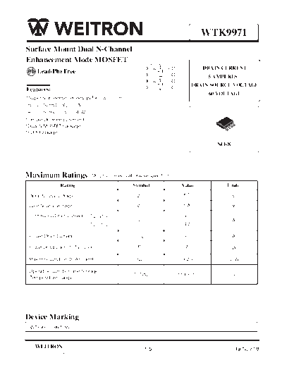
                                                                                WTK9971
Surface Mount Dual N-Channel
Enhancement Mode MOSFET
                                                                                 DRAIN CURRENT


                                                                   D1
 P b Lead(Pb)-Free


                                                         1
                                                    S1


                                                               8
                                                                   D1
                                                               7
                                                         2
                                                    G1
                                                                                   5 AMPERES


                                                                   D2
                                                    S2


                                                               6
                                                         3
                                                                              DRAIN SOURCE VOLTAGE


                                                                   D2
                                                    G2
Features:


                                                         4


                                                               5
                                                                                   60 VOLTAGE
*Super high dense cell design for low RDS(ON)
 RDS(ON)<50m @VGS = 10V
 RDS(ON)<60m @VGS = 4.5V
*Simple Drive Requirement
*Dual N MOSFET Package
*SO-8 Package                                                                           1


                                                                                     SO-8


Maximum Ratings (TA=25 C Unless Otherwise Specified)
                  Rating                        Symbol                  Value           Unite
  Drain-Source Voltage                           VDS                    60                  V
  Gate-Source Voltage                            VGS                    +
                                                                        - 20                V
  Continuous Drain Current (1) (TA =25


◦ Jabse Service Manual Search 2024 ◦ Jabse PravopisonTap.bg ◦ Other service manual resources online : FixyaeServiceinfo