Service Manuals, User Guides, Schematic Diagrams or docs for : . Electronic Components Datasheets Active components Transistors Wietron bss84

<< Back | Home

Most service manuals and schematics are PDF files, so You will need Adobre Acrobat Reader to view : Acrobat Download Some of the files are DjVu format. Readers and resources available here : DjVu Resources
For the compressed files, most common are zip and rar. Please, extract files with Your favorite compression software ( WinZip, WinRAR ... ) before viewing. If a document has multiple parts, You should download all, before extracting.
Good luck. Repair on Your own risk. Make sure You know what You are doing.


Image preview - the first page of the document
bss84


>> Download bss84 documenatation <<

Text preview - extract from the document
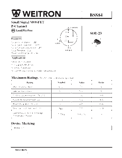
                                                                                   BSS84
Small Signal MOSFET
P-Channel                                                       3 DRAIN


                                                                                   SOT-23
Features:                                     1                                             3
*Low On-Resistance : 10                      GATE                                  1
*Low Input Capacitance: 30PF                                                           2
*Low Out put Capacitance : 10PF                                 2
*Low Threshole : 2.0V                                        SOURCE
*Fast Switching Speed : 2.5ns

 Application:
* DC to DC Converter
* Cellular & PCMCIA Card
* Cordless Telephone
* Power Management in Portable and Battery etc.


Maximum Ratings (TA=25 C Unless Otherwise Specified)
                   Rating                         Symbol                  Value            Unite
  Drain-Source Voltage                             VDSS                   50                    V
  Gate-Source Voltage                              VGS                    +
                                                                          -20                   V
  Continuous Drain Current (TA=25 C)                ID                    130               mA
  Pulsed Drain Current(tp 10us)                    IDM                    520               mA
  Power Dissipation (TA=25 C)                       PD                    225              mW
  Maximax Junction-to-Ambient                      R JA                   556               C/W

  Operating Junction and Storage
                                                  TJ, Tstg            -55 to 150                C
  Temperature Range


Device Marking
    BSS84=PD


     WEITRON
http://www.weitron.com.tw
             BSS84
Electrical Characteristics                  (TA=25 C Unless otherwise noted)
                Characteristic                           Symbol           Min          Typ      Max      Unit

Static (1)
 Drain-Source Breakdown Voltage                          V(BR)DSS                                         V
 VGS=0V, ID=250 uA                                                         50           -        -
 Gate-Source Threshold Voltage                            VGS (th)
 VDS=VGS, ID=1.0 mA                                                        0.8          -       2.0       V
 Gate-Source Leakage Current                               IGSS                                 +        uA
              +
 VDS=0V, VGS=-20V                                                              -        -       -60
 Zero Gate Voltage Drain Current
 VDS=25V, VGS=0V                                            IDSS               -        -       0.1      uA
 VDS=50V, VGS=0V                                                                                15
 Drain-Source On-Resistance
 VGS=5.0V, ID=100mA
                                                          rDS (on)             -        5.0     10

 Forward Transconductance                                   gfs            50               -        -   mS
 VDS=25V, ID=100mA, f=1.0KHZ


Dynamic
 Input Capacitance                                          Ciss               -        30           -
 VDS=5V, VGS=0V, f=1MHZ
 Output Capacitance                                                            -                     -
                                                            Coss                        10               PF
 VDS=5V, VGS=0V, f=1MHZ
 Reverse Transfer Capacitance
                                                            Crss               -        5.0          -
 VDS=5V, VGS=0V, f=1MHZ


Switching (2)
 Turn-On Time
                                                           td(on)              -        25       -        nS
 VDD =-15V, I D=-2.5A, R L =50
 Rise Time
                                                             tr                -        1.0      -
 VDD =-15V, I D=-2.5A, R L =50
 Turn-Off Time
                                                          td(off )             -        16       -        nS
 VDD =-15V, I D=-2.5A, R L =50
 Fall Time                                                                                       -
                                                             tf                -        8.0
 VDD =-15V, I D=-2.5A, R L =50
 Gate Charge                                                QT                 -       6000      -        PC

Source-Drain Diode Characteristics
 Continuous Current                                          IS                    -        -   0.130
                                                                                                          A
 Pulsed Current                                              I SM              -            -   0.520

 Forward Voltage (2)                                         VSD                   -    2.5          -    V

Note:
     1. Pulse Test : PW 300us, Duty Cycle 2%.
      2. Switching Time is Essentially Independent of Operating Temperature.


     WEITRON
http://www.weitron.com.tw
                                                                BSS84

                                                                                                     TYPICAL ELECTRICAL CHARACTERISTICS
                                                               0.6                                                                                                                                 0.5
                                                                         VDS = 10 V                                       25 C                                                                               TJ = 25 C                                   VGS = 3.5 V
                                                                                                                                                                                                  0.45
                                                               0.5
     I D , DRAIN CURRENT (AM PS)


                                                                                                                                                                I D , DRAIN CURRENT (AM PS)
                                                                                                                                                                                                   0.4                                                           3.25 V
                                                                                                             - 55 C
                                                                                                                               150 C
                                                                                                                                                                                                  0.35
                                                               0.4
                                                                                                                                                                                                   0.3                                                           3.0 V
                                                               0.3                                                                                                                                0.25
                                                                                                                                                                                                   0.2                                                        2.75 V
                                                               0.2
                                                                                                                                                                                                  0.15
                                                                                                                                                                                                                                                                 2.5 V
                                                                                                                                                                                                   0.1
                                                               0.1
                                                                                                                                                                                                  0.05                                                        2.25 V

                                                                0                                                                                                                                   0
                                                                     1           1.5       2         2.5      3           3.5          4                                                                 0    1      2    3         4   5     6    7     8         9      10
                                                                                  VGS , GATE- TO- SOURCE VOLTAGE (VOLTS)                                                                                           VDS , DRAIN- TO- SOURCE VOLTAGE (VOLTS)

                                                                                    FIG1. Transfer Characteristics                                                                                                  FIG2. On-Region Characteristics
              R DS(on) , DRAIN- TO- SOURCE RESISTANCE (OHMS)


                                                                                                                                                 R DS(on) , DRAIN- TO- SOURCE RESISTANCE (OHMS)


                                                                     9                                                                                                                               7
                                                                             VGS = 4.5 V                                                                                                                                                            150 C
                                                                                                                                                                                                   6.5       VGS = 10 V
                                                                     8                                                    150 C
                                                                                                                                                                                                     6
                                                                     7                                                                                                                             5.5

                                                                     6                                                                                                                               5
                                                                                                                                                                                                   4.5
                                                                     5                                                  25 C
                                                                                                                                                                                                     4                                                   25 C
                                                                     4                                                                                                                             3.5
                                                                                                                          - 55 C                                                                     3
                                                                     3                                                                                                                                                                                  - 55 C
                                                                                                                                                                                                   2.5
                                                                     2                                                                                                                               2
                                                                         0         0.1         0.2    0.3         0.4          0.5         0.6                                                           0         0.1        0.2       0.3       0.4        0.5          0.6
                                                                                           ID, DRAIN CURRENT (AM PS)                                                                                                       ID, DRAIN CURRENT (AM PS)
                                                                             FIG3. On-Resistance versus Drain Current                                                                                        FIG4. On-Resistance versus Drain Current


     WEITRON
http://www.weitron.com.tw
                                              BSS84


                                               2                                                                                                                                        8


                                                                                                                                                VGS , GATE-T O-SOURCE VOLTAGE (VOLTS)
       R DS(on), DRAIN-TO-SOURCE RESISTANCE


                                                                                                                                                                                                VDS = 40 V
                                              1.8                                                                    VGS = 10 V                                                         7       TJ = 25 C
                                                                                                                     ID = 0.52 A
                                              1.6                                                                                                                                       6
                    (NORMALIZED)


                                                                                                                                                                                        5
                                              1.4
                                                                                                                           VGS = 4.5 V
                                                                                                                                                                                        4
                                              1.2                                                                          ID = 0.13 A
                                                                                                                                                                                        3                               ID = 0.5 A
                                               1
                                                                                                                                                                                        2
                                              0.8
                                                                                                                                                                                        1
                                              0.6                                                                                                                                       0
                                                - 55            -5                                      45            95                 145                                                0            500             1000         1500   2000
                                                                TJ , JUNCTION TEMPERATURE ( C)                                                                                                               QT, TOTAL GATE CHARGE (pC)

                                                       FIG5. On-Resistance Variation with Temperature                                                                                                           FIG6. Gate Charge


                                                                                                             1
                                                                           I D , DIODE CURRENT (AMPS)


                                                                                                                     TJ = 150 C          25 C                                               -55 C
                                                                                                          0.1


                                                                                                         0.01


                                                                                                        0.001
                                                                                                                 0   0.5           1.0         1.5                                          2.0        2.5        3.0
                                                                                                                        VSD, DIODE FORWARD VOLTAGE (VOLTS)

                                                                                                                       FIG7. Body Diode Forward Voltage


     WEITRON
http://www.weitron.com.tw


◦ Jabse Service Manual Search 2024 ◦ Jabse PravopisonTap.bg ◦ Other service manual resources online : FixyaeServiceinfo