Service Manuals, User Guides, Schematic Diagrams or docs for : . Electronic Components Datasheets Active components Transistors Wietron c1815
<< Back | HomeMost service manuals and schematics are PDF files, so You will need Adobre Acrobat Reader to view : Acrobat Download Some of the files are DjVu format. Readers and resources available here : DjVu Resources
For the compressed files, most common are zip and rar. Please, extract files with Your favorite compression software ( WinZip, WinRAR ... ) before viewing. If a document has multiple parts, You should download all, before extracting.
Good luck. Repair on Your own risk. Make sure You know what You are doing.
Image preview - the first page of the document
>> Download c1815 documenatation <<
Text preview - extract from the document
C1815
NPN Plastic-Encapsulate Transistors
P b Lead(Pb)-Free
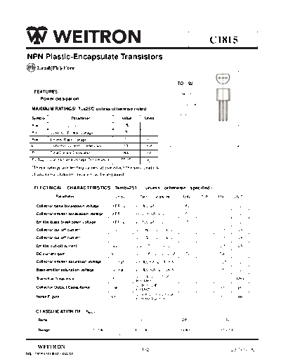
TO--92
FEATURES 1.EMITTER
Power dissipation
2.COLLECTOR
MAXIMUM RATINGS* TA=25 unless otherwise noted
3.BASE
Symbol Parameter Value Units
VCBO Collector-Base Voltage 60 V
1 2 3
VCEO Collector-Emitter Voltage 50 V
VEBO Emitter-Base Voltage 5 V
IC Collector Current -Continuous 150 mA
PD Total Device Dissipation 400 mW
TJ, Tstg Junction and Storage Temperature -55-150
*These ratings are limiting values above which the serviceability
of any semiconductor device may be impaired.
ELECTRICAL CHARACTERISTICSTamb=25 unless otherwise specified
Parameter Symbol Test conditions MIN TYP MAX UNIT
Collector-base breakdown voltage V(BR)CBO Ic= 100 uA, IE=0 60 V
Collector-emitter breakdown voltage V(BR)CEO Ic= 0. 1 mA, IB=0 50 V
Emitter-base breakdown voltage V(BR)EBO IE= 100 uA, IC=0 5 V
Collector cut-off current ICBO VCB= 60 V, IE=0 0.1 uA
Collector cut-off current ICEO VCE= 50 V, IB=0 0.1 uA
Emitter cut-off current IEBO VEB= 5 V, IC=0 0.1 uA
DC current gain hFE(1) VCE= 6 V, IC= 2mA 70 700
Collector-emitter saturation voltage VCE(sat) IC= 100mA, IB= 10 mA 0.25 V
Base-emitter saturation voltage VBE(sat) IC= 100 mA, IB= 10mA 1 V
VCE= 10 V, IC= 1mA
Transition frequency fT 80 MHz
f=30MHz
VCB=10V,IE=0
Collector Output Capacitance Cob 3.5 pF
f=1MHZ
VCE= 6 V, IC=0.1 mA
Noise Figure NF 10 dB
f =1KHz,RG=10K
CLASSIFICATION OF hFE(1)
Rank O Y GR BL
Range 70-140 120-240 200-400 350-700
WEITRON 1/2 23-Nov-06
http://www.weitron.com.tw
C1815
Typical Characteristics
WEITRON 2/2 23-Nov-06
http://www.weitron.com.tw
◦ Jabse Service Manual Search 2024 ◦ Jabse Pravopis ◦ onTap.bg ◦ Other service manual resources online : Fixya ◦ eServiceinfo