Service Manuals, User Guides, Schematic Diagrams or docs for : . Electronic Components Datasheets Active components Transistors Wietron mmun2111

<< Back | Home

Most service manuals and schematics are PDF files, so You will need Adobre Acrobat Reader to view : Acrobat Download Some of the files are DjVu format. Readers and resources available here : DjVu Resources
For the compressed files, most common are zip and rar. Please, extract files with Your favorite compression software ( WinZip, WinRAR ... ) before viewing. If a document has multiple parts, You should download all, before extracting.
Good luck. Repair on Your own risk. Make sure You know what You are doing.


Image preview - the first page of the document
mmun2111


>> Download mmun2111 documenatation <<

Text preview - extract from the document
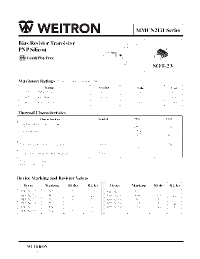
                                                                                           MMUN2111 Series

Bias Resistor Transistor                                                         COLLECTOR
                                                                                    3
PNP Silicon                                                   1
                                                                       R1                                       3
                                                             BASE      R2                             1
                                                                                                           2
                                                                                    2
                                                                               EMITTER
                                                                                                      SOT-23

Maximum Ratings ( TA=25 C unless otherwise noted)
                     Rating                                Symbol                           Value                       Unit
  Collector-Emitter Voltage                                 VCEO                             50                         Vdc
  Collector-Base Voltage                                     VCBO                             50                        Vdc
  Collector Current-Continuous                                IC                             100                        mAdc


Thermal Characteristics
                  Characteristics                          Symbol                         Max                   Unit
 Total Device Dissipation FR-5 Board
  (1)TA=25 C                                                 PD                           246 (1)                mW
   Derate above 25 C                                                                      400 (2)
                                                                                          1.5 (1)               mW/ C
                                                                                          2.0 (2)

 Thermal Resistance, Junction to Ambient                    R JA                           508                  C/W
                                                                                           311
 Junction and Storage, Temperature Range                   TJ,Tstg                      -55 to +150                 C

1.FR-4 @ minimum pad
2.FR-4 @ 1.0 l 1.0 inch Pad
            l


Device Marking and Resistor Values
     Device            Marking             R1(K)   R2(K)              Device             Marking      R1(K)         R2(K)
  MMUN2111               A6A                10      10               MMUN2130             A6G             1.0           1.0
  MMUN2112               A6B                22      22               MMUN2131             A6H             2.2           2.2
  MMUN2113               A6C                47      47               MMUN2132             A6J             4.7           4.7
  MMUN2114               A6D                10      47               MMUN2133             A6K             4.7            47
  MMUN2115               A6E                10                       MMUN2134             A6L             22             47
                                                    8 8


  MMUN2116               A6F                4.7


       WE ITR O N
http://www.weitron.com.tw
  MMUN2111 Series                                                                             WE IT R ON

Electrical Characteristics               (TA=25 C Unless Otherwise noted)
                                 Characteristics                       Symbol      Min   Typ    Max    Unit


Off Characteristics
 Collector-Emitter Breakdown Voltage                                                                   V
                                                                       V(BR)CEO    50    -       -
 (IC=2.0mA, IB =0)
 Collector-Base Breakdown Voltage
                                                                       V(BR)CBO    50    -       -      V
 (IC=10 uA ,IE=0)
 Collector-Base Cutoff Voltage
                                                                            ICBO    -     -     100    nA
 (VCB=50 V, I E =0)
 Collector-Emitter Cutoff Current                                           ICEO    -     -     500    nA
 (VCE=50V, I B =0)
 Emitter-Base Cutoff Current                         MMUN2111                       -     -     0.5
                                                                            IEBO                       mA
  (VEB=6.0V, IC =0)                                  MMUN2112                       -     -     0.2
                                                     MMUN2113                       -     -     0.1
                                                     MMUN2114                       -     -     0.2
                                                     MMUN2115                       -     -     0.9
                                                     MMUN2116                       -     -     1.9
                                                     MMUN2130                       -     -     4.3
                                                     MMUN2131                       -     -     2.3
                                                     MMUN2132                       -     -     1.5
                                                     MMUN2133                       -     -     0.18
                                                     MMUN2134                       -     -     0.13


On Characteristics
 Collector-Emitter Saturation Voltage                                  VCE(sat)           -            Vdc
                                                                                    -           0.25
 (I C=10mA, IB =0.3mA)
 (IC =10mA, I B =5mA) MMUN2130/MMUN2131
 (IC =10mA, IB =1mA) MMUN2115/MMUN2116
           MMUN2132/MMUN2133/MMUN2134

3. Pulse Test: Pulse Width < 300 us, Duty Cycle < 2.0%


      WEITRON
http://www.weitron.com.tw
 MMUN2111 Series                                                                         WE IT R ON

Electrical Characteristics              (TA=25 C Unless Otherwise noted)
                               Characteristics                        Symbol      Min   Typ   Max   Unit


On Characteristics (3)
 DC Current Gain                            MMUN2111                       h FE    35   60     -
 (VCE=10V, IC =5.0mA)                       MMUN2112                               60   100    -
                                            MMUN2113                               80   140    -
                                            MMUN2114                               80   140    -
                                            MMUN2115                              160   250    -
                                            MMUN2116                              160   250    -
                                            MMUN2130                              3.0   5.0    -
                                            MMUN2131                              8.0   15     -
                                            MMUN2132                               15   27     -
                                            MMUN2133                               80   140    -
                                            MMUN2134                               80   130    -

 Output Voltage(on)                                                        VOL                      Vdc
 (VCC=5.0V, VB =2.5V, R L =1.0k  )          MMUN2111                               -     -    0.2
                                            MMUN2112                               -     -    0.2
                                            MMUN2114                               -     -    0.2
                                            MMUN2115                               -     -    0.2
                                            MMUN2116                               -     -    0.2
                                            MMUN2130                               -     -    0.2
                                            MMUN2131                               -     -    0.2
                                            MMUN2132                               -     -    0.2
                                            MMUN2133                               -     -    0.2
                                            MMUN2134                               -     -    0.2
  (VCC=5.0V, VB =3.5V, R L =1.0k  )         MMUN2113                               -     -    0.2

 Output Voltage(off )                                                      VOH    4.9    -     -    Vdc
 (VCC =5.0V, VB =0.5V, R L =1.0k  )         MMUN2115
 (VCC =5.0V, VB =0.25V, R L =1.0k  )        MMUN2116
                                            MMUN2131
                                            MMUN2132
  (VCC=5.0V, VB =0.050V, R L =1.0k  )       MMUN2130

3. Pulse Test: Pulse Width 300 us, Duty Cycle 2.0%
                                            V
                        V


     WEITRON
http://www.weitron.com.tw
 MMUN2111 Series                                                                              WE IT R ON
Electrical Characteristics               (TA=25 C Unless Otherwise noted)
                                Characteristics                        Symbol       Min     Typ    Max     Unit

On Characteristics
 Input Resistor                                       MMUN2111               R1      7.0    10      13     k
                                                      MMUN2112                      15.4    22     28.6
                                                      MMUN2113                      32.9    47     61.1
                                                      MMUN2114                       7.0    10      13
                                                      MMUN2115                       7.0    10      13
                                                      MMUN2116                       3.3    4.7     6.1
                                                      MMUN2130                       0.7    1.0     1.3
                                                      MMUN2131                       1.5    2.2     2.9
                                                      MMUN2132                       3.3    4.7     6.1
                                                      MMUN2133                       3.3    4.7     6.1
                                                      MMUN2134                      15.4    22     28.6

 Resistor Ratio MMUNM2111/MMUN2112/MMUN2113                                 R1/R2    0.8    1.0     1.2
                MMUN2114                                                            0.17    0.21   0.25
                MMUN2115/MMUN2116                                                     -       -      -
                MMUN2130/MMUN2131/MMUN2132                                           0.8    1.0     1.2
                MMUN2133                                                            0.055   0.1    0.185

4. Pulse Test: Pulse Width < 300 us, Duty Cycle < 2.0 %


      WEITRON
http://www.weitron.com.tw
 MMUN2111 Series                                                                                                                                                                                                                            WE IT R ON
                                                                                                                 MMUN2111 Series
                                                                                                       TYPICAL ELECTRICAL CHARACTERISTICS
                                                                                                                   MMUN2114
    VCE(sat) , MAXIMUM COLLECT R VOLTAGE (VOLTS)


                                                             1                                                                                                                       180


                                                                                                                                              hFE , DC CURRENT GAIN (NORMALIZED)
                                                                         IC /IB =10                                                                                                                    VCE = 10V                                   TA =75 C
                                                                                                            TA = -25 C                                                               160
                                                                                                                                                                                                                                            25 C
                                                                                                                                                                                     140
                                                                                                                                 25 C
                                                     0.1                                                                                                                                                                                -25 C
                                                                                                                         75 C                                                        120
                             O


                                                                                                                                                                                     100

                                                                                                                                                                                              80
                                                    0.01                                                                                                                                      60

                                                                                                                                                                                              40
                                                                                                                                                                                              20

                                                   0.001                                                                                                                                      0
                                                                 0                     20            40           60                     80                                                        1    2   4      6     8 10 15 20 40 50 60 70               80   90 100
                                                                                        IC , COLLECTOR CURRENT (mA)                                                                                                    IC , COLLECTOR CURRENT (mA)

                                                                                      FIG.1 VCE(sat) versus IC                                                                                                         FIG.2 DC Current Gain

                                                   4.5                                                                                                                              100
                                                     4                                                               f = 1 MHz                                                                                         TA =75 C                         25C
                                                                                                                     lE = 0 V
                                                   3.5
                                                                                                                                                                IC , COLLECTOR CURRENT (mA)


                                                                                                                     TA = 25C
    Cob , CAPACITANCE (pF)


                                                                                                                                                                                                                                                -25 C
                                                     3

                                                   2.5
                                                                                                                                                                                              10
                                                     2
                                                   1.5

                                                     1
                                                                                                                                                                                                                                             VO = 5 V
                                                   0.5
                                                     0                                                                                                                                        1
                                                         0           2      4     6 8 10 15 20 25 30 35 40                       45 50                                                             0            2                4         6             8            10
                                                                                 VR , REVERSE BIAS VOL TAGE (VOLTS)                                                                                                     Vin , INPUT VOLTAGE (VOLTS)

                                                                                 FIG.3 Output Capacitance                                                                                          FIG.4 Output Current versus Input Voltage


                                                   10                                                                                                                                                                                            +12 V
                                                                 VO = 0.2V              TA = -25 C
                                                                                                            25 C
    V in , INPUT VOLTAGE (VOLTS)


                                                                                                     75 C                                                                                              Typic al A pplic ation
                                                                                                                                                                                                        for P NP B R Ts
                                                    1


                                                                                                                                                                                                                                                        LOAD


                                                   0.1
                                                         0                      10             20       30        40                50
                                                                                      IC , COLLECTOR CURRENT (mA)

                                                             FIG.5 Input Voltage versus Output Current                                                                                             FIG.6 Inexpensive, Unregulated Current Source


                  WEITRON
http://www.weitron.com.tw
  MMUN2111 Series


SOT-23 Package Outline Dimensions                                           Unit:mm


                                    A                       Dim Min Max
                                                             A  0.35 0.51
                                                             B  1.19 1.40
                        T OP V IE W         B   C            C  2.10 3.00
                                                             D  0.85 1.05
                                                             E  0.46 1.00
                                D
                                                             G  1.70 2.10
                            G
              E                                              H  2.70 3.10
                            H                                J  0.01 0.13
                                                             K  0.89 1.10
                                            K                L  0.30 0.61
                                                             M 0.076 0.25
                                                    L
                                        J               M


      WEITRON
http://www.weitron.com.tw


◦ Jabse Service Manual Search 2024 ◦ Jabse PravopisonTap.bg ◦ Other service manual resources online : FixyaeServiceinfo