Service Manuals, User Guides, Schematic Diagrams or docs for : . Electronic Components Datasheets Active components Transistors Vishay si3443dv

<< Back | Home

Most service manuals and schematics are PDF files, so You will need Adobre Acrobat Reader to view : Acrobat Download Some of the files are DjVu format. Readers and resources available here : DjVu Resources
For the compressed files, most common are zip and rar. Please, extract files with Your favorite compression software ( WinZip, WinRAR ... ) before viewing. If a document has multiple parts, You should download all, before extracting.
Good luck. Repair on Your own risk. Make sure You know what You are doing.


Image preview - the first page of the document
si3443dv


>> Download si3443dv documenatation <<

Text preview - extract from the document
                                                                                                                                         Si3443DV
                                                                                                                                 Vishay Siliconix

                                           P-Channel 2.5-V (G-S) MOSFET

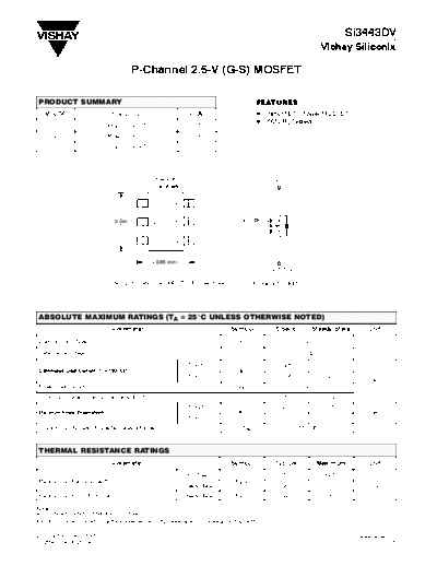
 PRODUCT SUMMARY                                                                                FEATURES
   VDS (V)                      rDS(on) (W)                         ID (A)                      D TrenchFETr Power MOSFET
                                                                                                D 100% Rg Tested
                             0.065 @ VGS = -4.5 V                    -4.5

      -20                    0.090 @ VGS = -2.7 V                    -3.8

                             0.100 @ VGS = -2.5 V                    -3.7


                                                     TSOP-6                                            (4) S
                                                    Top View


                                                    1         6


                                    3 mm                      5                       (3) G
                                                    2


                                                    3         4


                                                    2.85 mm
                                                                                                   (1, 2, 5, 6) D

                               Ordering Information: Si3443DV-T1--E3 (Lead Free)               P-Channel MOSFET


 ABSOLUTE MAXIMUM RATINGS (TA = 25_C UNLESS OTHERWISE NOTED)
                                 Parameter                                         Symbol               5 secs            Steady State        Unit
 Drain-Source Voltage                                                                VDS                               -20
                                                                                                                                                V
 Gate-Source Voltage                                                                 VGS                              "12

                                                                   TA = 25_C                              -4.5                    -3.4
 Continuous Drain Current (TJ = 150_C)a                                               ID
                                                                   TA = 70_C                              -3.6                    -2.7
                                                                                                                                                A
 Pulsed Drain Current                                                                 IDM                              -20

 continuous Source Current (Diode Conduction)a                                        IS                  -1.7                    -0.9

                                                                   TA = 25_C                               2.0                    1.1
 Maximum Power Dissipationa                                                           PD                                                       W
                                                                   TA = 70_C                               1.3                    0.7

 Operating Junction and Storage Temperature Range                                   TJ, Tstg                        -55 to 150                 _C


 THERMAL RESISTANCE RATINGS
                                 Parameter                                         Symbol              Typical               Maximum          Unit
                                                                   t v 5 sec                                50                    62.5
         Junction-to-Ambienta
 Maximum J
 M i         ti t A bi t                                                            RthJA
                                                                  Steady State                              90                    110          C/W
                                                                                                                                              _C/W
 Maximum Junction-to-Foot (Drain)                                 Steady State      RthJF                   22                    30

Notes
a. Surface Mounted on FR4 Board, t v 5 sec.
For SPICE model information via the Worldwide Web: http://www.vishay.com/www/product/spice.htm

Document Number: 71741                                                                                                                     www.vishay.com
S-32559--Rev. E, 29-Dec-03                                                                                                                             1
Si3443DV
Vishay Siliconix


 SPECIFICATIONS (TJ = 25_C UNLESS OTHERWISE NOTED)
                                    Parameter                        Symbol                  Test Condition                                       Min          Typ          Max           Unit

 Static
 Gate Threshold Voltage                                              VGS(th)               VDS = VGS, ID = -250 mA                                -0.6                       -1.4          V

 Gate-Body Leakage                                                     IGSS                 VDS = 0 V, VGS = "12 V                                                          "100           nA

                                                                                           VDS = -20 V, VGS = 0 V                                                             -1
 Zero Gate Voltage Drain Current                                       IDSS                                                                                                                mA
                                                                                      VDS = -20 V, VGS = 0 V, TJ = 70_C                                                       -5
 On-State Drain Currenta                                              ID(on)              VDS = -5 V, VGS = -4.5 V                                 -15                                     A
                                                                                          VGS = -4.5 V, ID = -4.5 A                                            0.050        0.065

 Drain-Source On-State Resistancea                                    rDS(on)              VGS = -2.7 V, ID = -3.8 A                                           0.070        0.090          W

                                                                                          VGS = -2.5 V, ID = -3.7 A                                            0.080        0.100

 Forward Transconductancea                                              gfs                VDS = -10 V, ID = -4.5 A                                             10                         S
 Diode Forward Voltagea                                                VSD                  IS = -1.7 A, VGS = 0 V                                             -0.8          -1.2          V

 Dynamicb
 Total Gate Charge                                                     Qg                                                                                       7.3           15
 Gate-Source Charge                                                    Qgs          VDS = -10 V, VGS = -4.5 V, ID = -4.5 A                                      2.0                       nC
 Gate-Drain Charge                                                     Qgd                                                                                      1.9
 Gate Resistance                                                        Rg                                                                          3                         15           W
 Turn-On Delay Time                                                   td(on)                                                                                    15            50
 Rise Time                                                              tr                                                                                      32            60
                                                                                           VDD = -10 V, RL = 10 W
 Turn-Off Delay Time                                                  td(off)        ID ^ -1.0 A, VGEN = -4.5 V, Rg = 6 W                                       50           100           ns
 Fall Time                                                              tf                                                                                      45            80
 Source-Drain Reverse Recovery Time                                     trr              IF = -1.7 A, di/dt = 100 A/ms                                          35            80

Notes
a. Pulse test; pulse width v 300 ms, duty cycle v 2%.
b. Guaranteed by design, not subject to production testing.


 TYPICAL CHARACTERISTICS (25_C UNLESS NOTED)

                                           Output Characteristics                                                                                Transfer Characteristics
                           20                                                                                                     20
                                                VGS = 5 thru 3.5 V     3V                                                                                        TC = -55_C

                           16                                                                                                     16                                 25_C
 I D - Drain Current (A)


                                                                                                        I D - Drain Current (A)


                                                                     2.5 V                                                                                                          125_C
                           12                                                                                                     12


                           8                                                                                                      8
                                                                       2V

                           4                                                                                                      4
                                                                     1.5 V

                           0                                                                                                      0
                                0      1          2          3           4      5                                                  0.0   0.5      1.0    1.5      2.0       2.5     3.0     3.5

                                       VDS - Drain-to-Source Voltage (V)                                                                       VGS - Gate-to-Source Voltage (V)


www.vishay.com                                                                                                                                                         Document Number: 71741
 2                                                                                                                                                                   S-32559--Rev. E, 29-Dec-03
                                                                                                                                                                                                Si3443DV
                                                                                                                                                                                    Vishay Siliconix

                TYPICAL CHARACTERISTICS (25_C UNLESS NOTED)
                                                    On-Resistance vs. Drain Current                                                                                            Capacitance
                                    0.20                                                                                                        1200
r DS(on) - On-Resistance ( W )


                                                                                                                                                1000
                                    0.16                                                                                                                                                 Ciss


                                                                                                               C - Capacitance (pF)
                                                                                       VGS = 2.7 V                                              800
                                    0.12

                                                                                                                                                600
                                               VGS = 2.5 V
                                    0.08
                                                                                       VGS = 4.5 V                                              400
                                                                                                                                                                        Coss

                                    0.04
                                                                                                                                                200

                                                                                                                                                           Crss
                                    0.00                                                                                                           0
                                           0            4            8           12           16         20                                            0           4            8         12            16         20

                                                                 ID - Drain Current (A)                                                                                VDS - Drain-to-Source Voltage (V)

                                                                    Gate Charge                                                                            On-Resistance vs. Junction Temperature
                                      5                                                                                                          1.6
                                                VDS = 10 V                                                                                                  VGS = 4.5 V
V GS - Gate-to-Source Voltage (V)


                                                ID = 4.5 A                                                                                                  ID = 4.5 A
                                                                                                               r DS(on) - On-Resistance (W)


                                      4                                                                                                          1.4
                                                                                                                         (Normalized)


                                      3                                                                                                          1.2


                                      2                                                                                                          1.0


                                      1                                                                                                          0.8


                                      0                                                                                                          0.6
                                           0                 2              4             6              8                                          -50      -25        0      25   50     75      100       125   150
                                                            Qg - Total Gate Charge (nC)                                                                                TJ - Junction Temperature (_C)


                                                  Source-Drain Diode Forward Voltage                                                                       On-Resistance vs. Gate-to-Source Voltage
                                     20                                                                                                         0.20


                                                                                                                                                0.16
                                                                                                               r DS(on) - On-Resistance ( W )
I S - Source Current (A)


                                     10                     TJ = 150_C                                                                                                                ID = 4.5 A
                                                                                                                                                0.12


                                                                                                                                                0.08

                                                                                      TJ = 25_C

                                                                                                                                                0.04


                                      1                                                                                                         0.00
                                       0.0        0.2        0.4      0.6       0.8    1.0         1.2   1.4                                           0           1            2         3              4         5
                                                        VSD - Source-to-Drain Voltage (V)                                                                              VGS - Gate-to-Source Voltage (V)


     Document Number: 71741                                                                                                                                                                             www.vishay.com
     S-32559--Rev. E, 29-Dec-03                                                                                                                                                                                          3
Si3443DV
Vishay Siliconix

     TYPICAL CHARACTERISTICS (25_C UNLESS NOTED)
                                                          Threshold Voltage                                                                      Single Pulse Power
                                  0.4
                                                                                                                                 25

                                  0.3
                                                                                                                                 20

                                  0.2
       VGS(th) Variance (V)


                                                          ID = 250 mA
                                                                                                                                 15


                                                                                                                     Power (W)
                                  0.1

                                                                                                                                 10
                                  0.0


                                                                                                                                  5
                                 -0.1


                                 -0.2
                                                                                                                                  0
                                     -50       -25    0       25     50      75   100    125     150
                                                                                                                                   10-2   10-1           1            10        100   600
                                                          TJ - Temperature (_C)                                                                       Time (sec)


                                                                          Normalized Thermal Transient Impedance, Junction-to-Ambient
                                        2

                                        1
                                               Duty Cycle = 0.5
Normalized Effective Transient
     Thermal Impedance


                                               0.2
                                                                                                                                            Notes:
                                               0.1
                                    0.1                                                                                                      PDM
                                               0.05
                                                                                                                                                     t1
                                                                                                                                                         t2
                                                                                                                                                                 t1
                                               0.02                                                                                         1. Duty Cycle, D =
                                                                                                                                                                 t2
                                                                                                                                            2. Per Unit Base = RthJA = 90_C/W
                                                                                                                                            3. TJM - TA = PDMZthJA(t)
                                                              Single Pulse                                                                  4. Surface Mounted
                                   0.01
                                            10-4              10-3                10-2                10-1                 1               10                    100            600
                                                                                               Square Wave Pulse Duration (sec)

                                                                            Normalized Thermal Transient Impedance, Junction-to-Foot
                                        2

                                        1
                                               Duty Cycle = 0.5
Normalized Effective Transient
     Thermal Impedance


                                               0.2

                                               0.1
                                    0.1
                                               0.05
                                               0.02


                                               Single Pulse
                                   0.01
                                            10-4                     10-3                        10-2                     10-1                       1                           10
                                                                                               Square Wave Pulse Duration (sec)


www.vishay.com                                                                                                                                                     Document Number: 71741
      4                                                                                                                                                          S-32559--Rev. E, 29-Dec-03
                                                                             Legal Disclaimer Notice
                                                                                                              Vishay

                                                  Disclaimer

All product specifications and data are subject to change without notice.

Vishay Intertechnology, Inc., its affiliates, agents, and employees, and all persons acting on its or their behalf
(collectively, "Vishay"), disclaim any and all liability for any errors, inaccuracies or incompleteness contained herein
or in any other disclosure relating to any product.

Vishay disclaims any and all liability arising out of the use or application of any product described herein or of any
information provided herein to the maximum extent permitted by law. The product specifications do not expand or
otherwise modify Vishay's terms and conditions of purchase, including but not limited to the warranty expressed
therein, which apply to these products.

No license, express or implied, by estoppel or otherwise, to any intellectual property rights is granted by this
document or by any conduct of Vishay.

The products shown herein are not designed for use in medical, life-saving, or life-sustaining applications unless
otherwise expressly indicated. Customers using or selling Vishay products not expressly indicated for use in such
applications do so entirely at their own risk and agree to fully indemnify Vishay for any damages arising or resulting
from such use or sale. Please contact authorized Vishay personnel to obtain written terms and conditions regarding
products designed for such applications.

Product names and markings noted herein may be trademarks of their respective owners.


Document Number: 91000                                                                                    www.vishay.com
Revision: 18-Jul-08                                                                                                    1


◦ Jabse Service Manual Search 2024 ◦ Jabse PravopisonTap.bg ◦ Other service manual resources online : FixyaeServiceinfo