Service Manuals, User Guides, Schematic Diagrams or docs for : . Electronic Components Datasheets Various RT9619

<< Back | Home

Most service manuals and schematics are PDF files, so You will need Adobre Acrobat Reader to view : Acrobat Download Some of the files are DjVu format. Readers and resources available here : DjVu Resources
For the compressed files, most common are zip and rar. Please, extract files with Your favorite compression software ( WinZip, WinRAR ... ) before viewing. If a document has multiple parts, You should download all, before extracting.
Good luck. Repair on Your own risk. Make sure You know what You are doing.


Image preview - the first page of the document
RT9619


>> Download RT9619 documenatation <<

Text preview - extract from the document
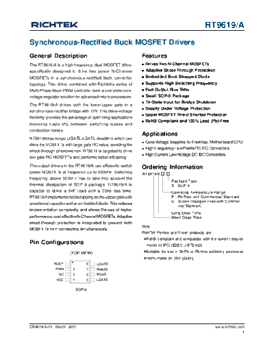
                                                                                                   RT9619/A

Synchronous-Rectified Buck MOSFET Drivers
General Description                                             Features
The RT9619/A is a high frequency, dual MOSFET driver              Drives Two N-Channel MOSFETs
specifically designed to drive two power N-Channel                Adaptive Shoot-Through Protection
MOSFETs in a synchronous-rectified buck converter                 Embedded Boot Strapped Diode
topology. This driver combined with Richtek's series of           Supports High Switching Frequency
Multi-Phase Buck PWM controller form a complete core-             Fast Output Rise Time
voltage regulator solution for advanced micro-processors.         Small SOP-8 Package
                                                                  Tri-State Input for Bridge Shutdown
The RT9619/A drives both the lower/upper gate in a
                                                                  Supply Under Voltage Protection
synchronous-rectifier bridge with 12V. This drive-voltage
                                                                  Upper MOSFET Direct Shorted Protection
flexibility provides the advantage of optimizing applications
                                                                  RoHS Compliant and 100% Lead (Pb)-Free
involving trade-offs between switching losses and
conduction losses.
                                                                Applications
RT9619A has longer UGATE/LGATE deadtime which can
                                                                  Core Voltage Supplies for Desktop, Motherboard CPU
drive the MOSFETs with large gate RC value, avoiding the
                                                                  High Frequency Low Profile DC-DC Converters
shoot-through phenomenon. RT9619 is targeted to drive
                                                                  High Current Low Voltage DC-DC Converters
low gate RC MOSFETs and performs better efficiency.
The output drivers in the RT9619/A can efficiently switch       Ordering Information
power MOSFETs at frequency up to 500kHz. Switching              RT9619/A
frequency above 500kHz has to take into account the
                                                                                Package Type
thermal dissipation of SOP-8 package. RT9619/A is                               S : SOP-8
capable to drive a 3nF load with a 30ns rise time.                              Operating Temperature Range
RT9619/A implements bootstrapping on the upper gate with                        P : Pb Free with Commercial Standard
                                                                                G : Green (Halogen Free with Commer-
an external capacitor and an embedded diode. This reduces                           cial Standard)
implementation complexity and allows the use of higher
                                                                                Long Dead Time
performance, cost effective N-Channel MOSFETs. Adaptive                         Short Dead Time
shoot-through protection is integrated to prevent both
                                                                Note :
MOSFETs from conducting simultaneously.
                                                                RichTek Pb-free and Green products are :
                                                                  RoHS compliant and compatible with the current require-
Pin Configurations                                                ments of IPC/JEDEC J-STD-020.

                       (TOP VIEW)                                 Suitable for use in SnPb or Pb-free soldering processes.
                                                                  100% matte tin (Sn) plating.
              BOOT               8     UGATE
               PWM       2       7     PHASE
                 NC      3       6     PGND
               VCC       4       5     LGATE

                             SOP-8


DS9619/A-04 March 2007                                                                                     www.richtek.com
                                                                                                                         1
2
www.richtek.com
                                                                                                                                                                                                                         RT9619/A


                                                                     L1
                                                                   2.2uH
                                  ATX_12V                                                                                              VIN
                                                                                                                                                                                           Typical Application Circuit


                                            C8        C9          C10              C11        C12             C13          C14
                                            10uF      10uF        1000uF           1000uF     1000uF          10uF         10uF

                                                                                                            C2
                                                                                                   R2       1uF
                                                                                   D1              1

                                                                                           1
                                                             R1                          BOOT                        R3
                                                             10                                         8            2.2
                                            ATX_12V                            4 VCC
                                                                                            UGATE                                 Q1
                                                                         C1
                                                                         1uF                                                                  L2
                                                                                        RT9619/A
                                                                                                        7                                    1uH
                                                                               3             PHASE                                                                                 VCORE
                                                                                                                                                   +
                                                                                                                                                            +
                                                                                                                                                                     +
                                                                                                                                                                            +


                                                                                   NC
                                                                                                                     R4                R5
                                                                               2                        5            0                 2.2         C4       C5       C6     C7
                                                                   PWM             PWM       LGATE                                Q2               2200uF   2200uF   10uF   10uF
                                                                                                                                       C3
                                                                                         PGND                                          3.3nF
                                                                                           6


         DS9619/A-04 March 2007
                                                                                                             RT9619/A
Functional Pin Description
Pin No.    Pin Name                                                  Pin Function
   1      BOOT                 Floating bootstrap supply pin for upper gate drive.
   2      PWM                  Input PWM signal for controlling the driver.
   3      NC                   No Connection Pin.
   4      VCC                  +12V Supply Voltage.
   5      LGATE                Lower Gate Drive Output. Connected to gate of low-side power N-Channel MOSFET.
   6      PGND                 Common Ground.
                               Connected this pin to the source of the high-side MOSFET and the drain of the low-side
   7      PHASE
                               MOSFET.
   8      UGATE                Upper Gate Drive Output. Connected to gate of high-side power N-Channel MOSFET.


Function Block Diagram
                                                VCC


                      Internal
                         5V
                                                POR
                           R
                                                                                                              BOOT
                                   Tri-State
          PWM                       Detect                                    Shoot-Through
                                                                                                              UGATE
                                                                                Protection
                           R


                                                                              Turn off Detect                 PHASE

                                                                                                      VCC

                                                                              Shoot-Through
                                                                                Protection                    LGATE
                                                                                                              PGND


Timing Diagram


                PWM
                            tpdlLGATE

            LGATE                       90%
                                                                               tpdlUGATE
                                               2V                                                       2V


                                                                                           90%
                                                      2V                                         2V
            UGATE

                                               tpdhUGATE                                         tpdhLGATE


DS9619/A-04 March 2007                                                                                         www.richtek.com
                                                                                                                             3
RT9619/A
Absolute Maximum Ratings                                 (Note 1)
 Supply Voltage, VCC -------------------------------------------------------------------------------------         -0.3V to 15V
 BOOT to PHASE -----------------------------------------------------------------------------------------           -0.3V to 15V
 BOOT to GND
 DC ------------------------------------------------------------------------------------------------------------   -0.3V to VCC + 15V
 < 200ns -----------------------------------------------------------------------------------------------------     -0.3V to 42V
 PHASE to GND
 DC ------------------------------------------------------------------------------------------------------------   -5V to 15V
 < 200ns -----------------------------------------------------------------------------------------------------     -10V to 30V
 LGATE
 DC ------------------------------------------------------------------------------------------------------------   GND - 0.3V to VCC + 0.3V
 < 200ns -----------------------------------------------------------------------------------------------------     -2V to VCC + 0.3V
 UGATE ------------------------------------------------------------------------------------------------------      VPHASE - 0.3V to VBOOT + 0.3V
 < 200ns -----------------------------------------------------------------------------------------------------     VPHASE - 2V to VBOOT + 0.3V
 PWM Input Voltage --------------------------------------------------------------------------------------          GND - 0.3V to 7V
 Power Dissipation, PD @ TA = 25


◦ Jabse Service Manual Search 2024 ◦ Jabse PravopisonTap.bg ◦ Other service manual resources online : FixyaeServiceinfo