Service Manuals, User Guides, Schematic Diagrams or docs for : . Various DVD Power Supply Schematics DVDR985_Philips
<< Back | HomeMost service manuals and schematics are PDF files, so You will need Adobre Acrobat Reader to view : Acrobat Download Some of the files are DjVu format. Readers and resources available here : DjVu Resources
For the compressed files, most common are zip and rar. Please, extract files with Your favorite compression software ( WinZip, WinRAR ... ) before viewing. If a document has multiple parts, You should download all, before extracting.
Good luck. Repair on Your own risk. Make sure You know what You are doing.
Image preview - the first page of the document
>> Download DVDR985_Philips documenatation <<
Text preview - extract from the document
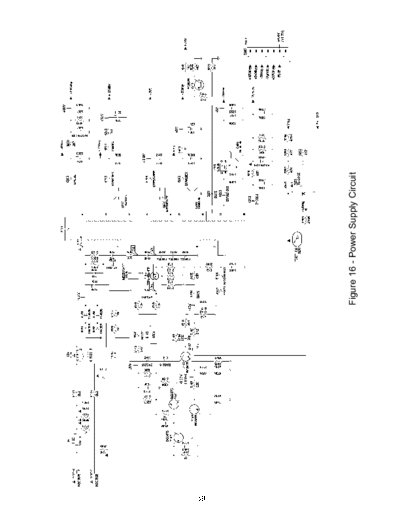
39
     Figure 16 - Power Supply Circuit
Power Supply                                            components and large enough to turn On 7140,
                                                        7125 is turned Off by 7140. Diodes 6130, 6131
                                                        and 6132 protect the control circuit in case of
This unit uses a stand alone Switch Mode Power
                                                        failure of the MOSFET by providing an upperlimit
Supply, SMPS. A MOSFET transistor turns On
                                                        to the voltage that can remain on the source of
and Off in an oscillator fashion, driving a trans-
                                                        the MOSFET.
former. The primary half of the supply uses a Hot
Ground. The primary side of the circuit provides
                                                        Coarse Regulation
drive and coarse control of the power supply.
                                                        The positive portion of the signal on Pins 7 and 8
The secondary side of the circuit rectifies and fil-
                                                        will be rectified via R3150 and D6140, charging
ters the output of the transformer to produce
                                                        C2140 via R3140. In time, the voltage on C2140
many output voltages. It uses a cold ground, sig-
                                                        will reach 15 to 20Vdc. This value depends on
nal ground system. Two of the output voltages
                                                        the value of the Mains voltage and the load. The
are monitored for precise regulation. The 12Vdc
                                                        negative portion of the signal on Pins 7 and 8
is supplied to the anode of the Optic Coupler's
                                                        will be rectified via R3150 and D6142. This will
diode, and the 5Vdc Standby is feed to the
                                                        charge C2151 to approximately -15Vdc. This is
Shunt Regulator. The regulation path includes an
                                                        used as a regulation supply.
Optic Coupler to accommodate the different
grounding systems.
                                                        The control circuit consists of T7140, D6141,
                                                        C2144, C2145, C2147, R3147, and 3148. This
Circuit Description
                                                        circuit controls the conduction time and the
                                                        switching frequency of the MOSFET. It switches
AC Input Circuit
                                                        Off the MOSFET as soon as the voltage on the
Refer to Figure 16. The input circuit consists of
                                                        source of T7125 reaches a certain value. This
a lightning protection circuit and an EMI filter.
                                                        value depends on the error voltage at the emitter
The lightning protection circuit consists of
                                                        of T7140, which can be a negative (+/- 0.6V).
R3120, spark gaps 1124 and 1125. L5110,
                                                        The voltage fed back by the regulation circuit
L5115, C2120 and L5121 form the EMI filter. It
                                                        defines this error voltage.
prevents noise coming in or out through the
mains. The AC input is rectified by diodes 6151,
                                                        Precise Regulation
6152, 6153, 6154, and filtered by C2126. The
                                                        The regulation circuit consists of an Optic-
voltage on C2126 is approximately 155V. It can
                                                        Coupler, 7200, 7251, and a voltage divider net-
vary from 150V to 160V, depending on the AC
                                                        work. The Optic-Coupler isolates the Hot Ground
input voltage.
                                                        referenced voltage on the emitter of 7140 from
                                                        the Cold Ground referenced voltage on 7251.
Start Circuit
                                                        7251, a Shunt Regulator, has two component
This circuit consists of R3125, 3126, R3139,
                                                        characteristics. It is a very stable and accurate
R3141, C2140, and R3132. When the power
                                                        reference diode and a high gain amplifier.
plug is connected to AC, the MOSFET 7125 will
start conducting as soon as the gate voltage
                                                        7251 will conduct from cathode to anode when
reaches the threshold value. A current starts to
                                                        the reference is higher than the internal refer-
flow in the primary winding of 5125, Pins 2 and
                                                        ence voltage of about 2.5Vdc. If the reference
4. The MOSFET will be fed forward via the wind-
                                                        voltage is lower, the cathode current is almost
ing connected to Pins 7 and 8 by R3150 and
                                                        zero. The cathode current flows through the LED
C2146. While the MOSFET is conducting, ener-
                                                        of the Optic-Coupler, controlling the current
gy is building up in the transformer. The current
                                                        through the transistor portion of the Optic-
flow through the MOSFET is sensed by R3133,
                                                        Coupler. The collector current of 7200 will adjust
3134, and 3135. When the current level rises
                                                        the feedback level of the error voltage at the
high enough to provide a voltage drop on these
                                                        emitter of T7140.

                                                       40
Overcurrent Protection Circuit                                Fluorescent Display driver
This circuit consists of R3145, C2143, a thyristor
circuit formed by T7141 and T7143, R3143 and                  Monitoring the keyboard matrix
R3142. When the output is shortened, the cur-
rent through the FET will produce a large voltage             Decoding the remote control commands
drop across the source resistors of the FET. That             from the infrared receiver, 6170.
voltage turns On 7140 and 7143. The thyristor
circuit will start to conduct and switch Off the              Activation of the display
supply voltage to C2140. This switches Off the
drain current of the MOSFET, 7125. The start cir-       The Fluorescent Tube operates using a grid and
cuit will try to start up the power supply again. If    segment scanning matrix. AC is supplied by a
the short still exists, the complete start and stop     switching regulator consisting of 7151, 7152,
sequence will repeat. The power supply is in a          7153, and 5153. With AC supplied, the micro-
hiccup mode and is ticking.                             computer scans the elements in the tube to
                                                        determine what segments light up. The system
Overvoltage Protection Circuit                          clock is generated with the 12MHz crystal, 1153.
This circuit consists of R3149, D6144, 6143,
R3144, C2142 and T7142. If the regulation cir-          Keyboard Matrix
cuit does not function due to an error in the con-      There are 11 different keys on the display board.
trol loop, the regulated output voltage will            A resistor network is used to generate a specific
increase. This overvoltage is sensed on the hot         voltage value, depending on the key pressed, via
ground side of the transformer at Pins 7 and 8.         the resistors 3186-90, 3145, 3197, 3177-3178,
When an overvoltage is detected, the circuit will       3197, and 3180. This RTL data (voltage Level) is
activate the thyristor circuit T7141 and 7142. The      sent to 7156 on Pins 17, 18, 19, and 20.
power supply will be shutdown as long as the            Pressing keys simultaneously may lead to unde-
error in the control loop is present.                   sired functions!

Secondary Rectifier/Smoothing Circuit
There are six Rectifier/Smoothing circuits on the
secondary side. Each supply voltage depends on
the number of windings in the transformer. From
these circuits, several voltages are derived and
fed to three connectors. The following voltages
are present at the output: 33Vdc, 12Vdc, 3.9Vdc,
and 5Vdc Stby, -5Vdc Stby, and -33Vdc Vgnstby.
The +12V is switched Off by the STBY_Ctrl sig-
nal, ION. The -33Vdc is dedicated to the Front
Panel Fluorescent Tube as a grid supply. The
FLYB signal is used as a Power Fail and mea-
surement signal.


Front Panel
The main elements of the Front Panel are the
microcomputer, 7156, the Display Tube, and the
keyboard. Refer to Figure 18. 7156 is an 8 bit
microcomputer fitted with 96kB ROM and 3kB
RAM and is responsible for the following func-
tions:
                                                              Figure 17 - RTL Voltage Chart
                                                       41
◦ Jabse Service Manual Search 2024 ◦ Jabse Pravopis ◦ onTap.bg ◦ Other service manual resources online : Fixya ◦ eServiceinfo