Service Manuals, User Guides, Schematic Diagrams or docs for : . Various SONIC SENS630_SENS670

<< Back | Home

Most service manuals and schematics are PDF files, so You will need Adobre Acrobat Reader to view : Acrobat Download Some of the files are DjVu format. Readers and resources available here : DjVu Resources
For the compressed files, most common are zip and rar. Please, extract files with Your favorite compression software ( WinZip, WinRAR ... ) before viewing. If a document has multiple parts, You should download all, before extracting.
Good luck. Repair on Your own risk. Make sure You know what You are doing.


Image preview - the first page of the document
SONIC SENS630_SENS670


>> Download SONIC SENS630_SENS670 documenatation <<

Text preview - extract from the document
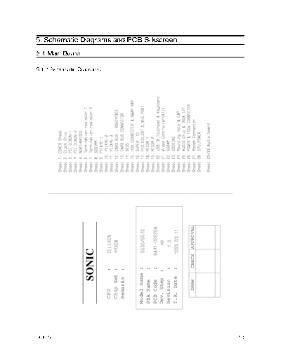
S630/S670
                                                                       5-1 Main Board


                   SONIC
                                            5-1-1 Schematic Diagrams


             CPU      :
             Chip Set :
             Remarks :


            Model Name   :
            PBA Name     :
            PCB Code     :
            Dev. Step    :
            Revision     :
                                                                                        5 Schematic Diagrams and PCB Silkscreen


            T.R. Date    :


                DRAW     CHECK   APPROVAL


5-1
5-2
                   4                                                             3                                                2         1


            D                                                                                                                                   D


                                                                                                                W48S87-72HTR(1209-001181)


            C                                                                                                                                   C
                                                                                                                                                                                                              5 Schematic Diagrams and PCB Silkscreen


                                                                                     KQT
                                                                                                                                                    5-1-1(a) Main Board Schematic Sheet 2 of 28(Clock Chip)


            B                                                                                                                                   B


                1) Don't place Clock chip near PCB edge. Place near PCB center and mounting hole.
                   Make the clock generator area more "clean"
                2) Every power pins have a decoupling CAP direct connect it.
                   Make the shortest trace.
                3) Ground pin directly connect to ground plane.
                4) Make trace of power pin and ground pin short and wider than width of chip pad.
                5) Don't place via between clock chip power pin and decoupling CAP.
                6) Clock trace must have damping resistor and filter Capacitor near to clock chip output pin.
            A   7) No other signal trace across through the clock generator area.                                                               A
                   Including crystal, clock chip, decoupling capacitor, damping and filter.


                   4                                                             3                                                2         1


S630/S670
                4                    3                                                       2                                              1


S630/S670
            D                                                                                                                                                      D


            C                                                                                                                                                      C


                                                                                                                                                Refer To Table A


                    3-B4


                                    1%
                           OPTION

            B                                                                                                                                                      B
                                                                                                                                                                       5-1-1(b) Main Board Schematic Sheet 3 of 28(PII DIXON-1)


                                                                                        ITP I/F Board Signals

                                                                                         1   PCORE
                                                                                         2   CLK2_HCLK1
                                                                                         3   CPU2_TCK
                                                                                         4   CPU_TMS                Table A (ITP Debugging Option)
                                                                                         5   CPU2_TRST*
                                                                                         6   P2.5V
                                                                                         7   CPU2_PREQ*         To use ITP Debugging Mode, Do not Install
                                                                                         8   CPU1_PRDY*
                                                                                         9   CPU2_TDO
                                                                                        10   CPU2_TDI           the resistors on the TCK, TDI, TMS.
                                                                                        11   GND
                                     Core Frequency to System Bus Ratio Configuration   12   CPU1_CPURST*       And connect ITP I/F Board.
                                                                                        13   GND


            A                                                                                                                                                      A


                                                    ON = L , OFF = H


                4                    3                                                       2                                              1


5-3
                                                                                                                                                                                                                                  5 Schematic Diagrams and PCB Silkscreen
5 Schematic Diagrams and PCB Silkscreen


5-1-1(c) Main Board Schematic Sheet 4 of 28(PII DIXON-2)
             D


                                    C


                                                     B


                                                                     A
  1


                                                                              1
  2


                                                                              2
  3


                                                                              3
                                                           ADM1021
  4


                                                                              4
             D


                                    C


                                                     B


                                                                     A


5-4                                                                      S630/S670
                                                                                          5 Schematic Diagrams and PCB Silkscreen


5-1-1(d) Main Board Schematic Sheet 5 of 28(NORTHBRIDGE)
            D


                                                                                      C


                                                                                           B


                                                                                                                  A
  1


                                                                                                                             1
            Decoupling Caps should be placed

                                               at the corner of the 443BX
  2


                                                                                                                             2
  3


                                                                                                                             3
                                                                            82443DX
  4


                                                                                                                             4
            D


                                                                                      C


                                                                                           B


                                                                                                                  A


S630/S670                                                                                                                     5-5
5-6
                           4                      3   2   1


            D                                                 D


            C   443DX Strapping Options                       C
                                                                                                                                        5 Schematic Diagrams and PCB Silkscreen


                   Enable Mobile Low Power GTL+

                                     5-C3

                      Disable AGP Mode

                                     5-C3


                    Enable Quick Start Mode

                                     5-C3


                     Disable Pipelining
            B                                                 B
                                     5-C3
                                                                  5-1-1(e) Main Board Schematic Sheet 6 of 28(Termination resistor 1)


            A                                                 A


                           4                      3   2   1


S630/S670
                                                      5 Schematic Diagrams and PCB Silkscreen


5-1-1(f) Main Board Schematic Sheet 7 of 28(Termination resistor 1)
                   D


                                 C


                                                       B


                                                                              A
  1


                                                                                         1
            3-B1
  2


                                                                                         2
  3


                                                                                         3
  4


                                                                                         4
                   D


                                 C


                                                       B


                                                                              A


S630/S670                                                                                 5-7
5 Schematic Diagrams and PCB Silkscreen


5-1-1(g) Main Board Schematic Sheet 8 of 28(SODIMM)
             D


                                           C


                                                                 B


                                                                     A
                                                        OPTION
  1


                                                                              1
                                  OPTION
  2


                                                                              2
                                                        OPTION
  3


                                                                              3
                                               OPTION
  4


                                                                              4
             D


                                           C


                                                                 B


                                                                     A


5-8                                                                      S630/S670
                                                    5 Schematic Diagrams and PCB Silkscreen


5-1-1(h) Main Board Schematic Sheet 9 of 28(PIIX4E-1)
            D


                                C


                                                        B


                                                                            A
  1


                                                                                       1
  2


                                                                                       2
  3


                                                                                       3
  4


                                                                                       4
            D


                                C


                                                        B


                                                                            A


S630/S670                                                                               5-9
5 Schematic Diagrams and PCB Silkscreen


5-1-1(i) Main Board Schematic Sheet 10 of 28(PIIX4E-2)
             D


                                    C


                                                         B


                                                                                         A
  1


                                                                                                  1
                                                             All components in the Box
                                                             need to be placed
                                                             near PIIX4E
  2


                                                                                                  2
  3


                                                                                                  3
  4


                                                                                                  4
             D


                                    C


                                                         B


                                                                                         A


5-10                                                                                         S630/S670
                    4                             3                              2              1


S630/S670
            D                                                                                                       D


                           PIIX4E Resource Table


                  PCI BUS Request                  IDSEL
            C   PREQ 0    Docking            PIIX4E        AD 18                                                    C
                PREQ 1    VIDEO              CardBus       AD 19
                PREQ 2    Modem              Reserved
                PREQ 3    CardBus            Audio         AD 23
                PREQ 4    Audio              Modem         AD 24
                                             VIDEO         AD 16
                                       **Docking CardBus   AD 20           CBS

                                                                           DCK

                                                                           AUD
                                                                            MDM      Wired_OR
                PC/PCI DMA Request      Programmable Interrupt Request
                                        INTA*    Docking, CardBus, MODEM
                                                                                                                        5-1-1(j) Main Board Schematic Sheet 11 of 28(PIIX4E-3)


                 PREQA*     Not used
            B    PREQB*     Audio       INTB*    Docking, Cardbus, LAN                                              B
                 PREQC*     Not used    INTC*    Video, Audio
                                        INTD*    USB


                                                                                                    STRAIGHT type


            A                                                                                                       A


                    4                             3                              2              1


5-11
                                                                                                                                                                                 5 Schematic Diagrams and PCB Silkscreen
5 Schematic Diagrams and PCB Silkscreen


5-1-1(k) Main Board Schematic Sheet 12 of 28(CARD BUS: RB5C478II)
             D


                                    C


                                                   B


                                                                    A
  1


                                                                             1
  2


                                                                             2
  3


                                                                             3
  4


                                                                             4


                      13-D3
             D


                                    C


                                                   B


                                                                    A


5-12                                                                    S630/S670
                4   3           2           1


S630/S670
            D                                   D


                        12-A3       12-C4
                                    12-C4
                                    12-C4
                                    12-C4
                                    12-C4
                                    12-C4
                                    12-C4
                                    12-D4
                                    12-D4
                                    12-C4
                                    12-C4
                                    12-C4
                                    12-C4


                        12-A3       12-C2
                                    12-C2
                                    12-C2
                                    12-C2
                                    12-C2
            C                       12-C2       C
                                    12-C2
                                    12-D2
                                    12-D2
                                    12-C2
                                    12-C2
                                    12-C2
                                    12-C2


            B                                   B
                                                    5-1-1(l) Main Board Schematic Sheet 13 of 28(CARD BUS CONNECTOR)


            A                                   A


                4   3           2           1


5-13
                                                                                                                       5 Schematic Diagrams and PCB Silkscreen
5 Schematic Diagrams and PCB Silkscreen


5-1-1(m) Main Board Schematic Sheet 14 of 28(BIOS)
             D


                                    C


                                                     B


                                                         A
  1


                                                                  1
  2


                                                                  2
  3


                                                                  3
  4


                                                                  4
             D


                                    C


                                                     B


                                                         A


5-14                                                         S630/S670
                                                     5 Schematic Diagrams and PCB Silkscreen


5-1-1(n) Main Board Schematic Sheet 15 of 28(HDD CONNECTOR & SWAP BAY)
            D


                             C


                                                      B


                                                                             A
  1


                                                                                              1
  2


                                                                                              2
                                                                              HDD CONNECTOR
  3


                                                                                              3
                                          SWAP BAY
  4


                                                                                              4
            D


                             C


                                                      B


                                                                             A


S630/S670                                                                                     5-15
5 Schematic Diagrams and PCB Silkscreen


5-1-1(o) Main Board Schematic Sheet 16 of 28(SUPER IO)
             D


                                    C


                                                            B


                                                                                           A
  1


                                                                                                    1
  2


                                                                                                    2
                                          OPTION


                                                                         OPTION
                                                   OPTION


                                                                                  OPTION
  3


                                                                                                    3
                                                                OPTION
  4


                                                                                                    4
             D


                                    C


                                                            B


                                                                                           A


5-16                                                                                           S630/S670
                                                    5 Schematic Diagrams and PCB Silkscreen


5-1-1(p) Main Board Schematic Sheet 17 of 28(PIO, SIO, CRT, S_VHS PORT)
            D


                               C


                                                        B


                                                                            A
                                                  MONITOR
                                   S_VHS
  1


                                                                                       1
  2


                                                                                       2
                                           SIO


                                                                     PIO
  3


                                                                                       3
            HIN211
  4


                                                                                       4
            D


                               C


                                                        B


                                                                            A


S630/S670                                                                              5-17
5 Schematic Diagrams and PCB Silkscreen


5-1-1(q) Main Board Schematic Sheet 18 of 28(MICOM 1)
             D


                                    C


                                                   B


                                                                                          A
  1


                                                                                                   1
  2


                                                                                                   2
  3


                                                                                                   3
                                                        KQT


                                                              Using of another purpose.
  4


                                                                                                   4
             D


                                    C


                                                   B


                                                                                          A


5-18                                                                                          S630/S670
                                                  5 Schematic Diagrams and PCB Silkscreen


5-1-1(u) Main Board Schematic Sheet 19 of 28(MICOM 2)
            D


                               C


                                                   B


                                                                          A
  1


                                                                                     1
  2


                                                                                     2
  3


                                                                                     3
  4


                                                                                     4
            D


                               C


                                                   B


                                                                          A


S630/S670                                                                            5-19
5 Schematic Diagrams and PCB Silkscreen


5-1-1(r) Main Board Schematic Sheet 20 of 28(USB, IR, Touchpad & Keyboard)
             D


                                    C


                                                                 B


                                                                         A
                                                                 PS/2
  1


                                                                                  1
                  Key B'd
  2


                                                                                  2
                                                 LED, TouchPad
  3


                                                                                  3
  4


                                                                                  4
             D


                                    C


                                                                 B


                                                                         A


5-20                                                                         S630/S670
                                                               5 Schematic Diagrams and PCB Silkscreen


5-1-1(s) Main Board Schematic Sheet 21 of 28(Video Controller[ATI])
                     D


                                 C


                                                                B


                                                                                       A
  1


                                                                                                  1
  2


                                                                                                  2
  3


                                                                                                  3
            option


                                                                            33
                                      SELECTION
                                                  ALL IN ONE
                                                   FLEX BAY
                                      SW2
                                                  OFF
                                                  ON
  4


                                                                                                  4
                                      SELECTION

                                                  SVGA
                                                  XGA
                                      SW1
                                                  OFF
                                                  ON
                     D


                                 C


                                                                B


                                                                                       A


S630/S670                                                                                         5-21
5 Schematic Diagrams and PCB Silkscreen


5-1-1(t) Main Board Schematic Sheet 22 of 28(SGRAM)
             D


                                                  C


                                                      B


                                                          A
                                  LCD CONNECTOR
  1


                                                                   1
  2


                                                                   2
  3


                                                                   3
  4


                                                                   4
             D


                                                  C


                                                      B


                                                          A


5-22                                                          S630/S670
                                                  5 Schematic Diagrams and PCB Silkscreen


5-1-1(u) Main Board Schematic Sheet 23 of 28(DOCKING)
            D


                               C


                                                   B


                                                                          A
  1


                                                                                     1
  2


                                                                                     2
  3


                                                                                     3
  4


                                                                                     4
            D


                               C


                                                   B


                                                                          A


S630/S670                                                                            5-23
5 Schematic Diagrams and PCB Silkscreen


5-1-1(v) Main Board Schematic Sheet 24 of 28(Mounting Hole & CAP)
             D


                                    C


                                                   B


                                                                     A
                                                            MP
                                                            1.0
  1


                                                                              1
                                                            990311
  2


                                                                              2
  3


                                                                              3
  4


                                                                              4
             D


                                    C


                                                   B


                                                                     A


5-24                                                                     S630/S670
                                                         5 Schematic Diagrams and PCB Silkscreen


5-1-1(w) Main Board Schematic Sheet 25 of 28(AUDIO Chip & IRDA I/F)
            D


                                     C


                                                          B


                                                                                                A
                                                                          Audio I/F connector
  1


                                                                                                           1
                              use 3.3V


                                                OPTION
  2


                                                                                                           2
  3


                                                                                                           3
                                                                                                STRAIGHT
                                                                                 INTERNAL MIC
                ES1978S
  4


                                                                                                           4
            D


                                     C


                                                          B


                                                                                                A


S630/S670                                                                                                  5-25
5 Schematic Diagrams and PCB Silkscreen


5-1-1(x) Main Board Schematic Sheet 26 of 28(POWER & FDDs CONNECTER)
             D


                                    C


                                                                                           B


                                                                                                                                         A
  1


                                                                                                                                                       1
                                                                                               Charger board connector
                                          DC/DC board connector
  2


                                                                                                                                                       2
                                                                  External FDD connector
  3


                                                                                                                                                       3
                                                                                                                         Internal FDD connector
  4


                                                                                                                                                       4
             D


                                    C


                                                                                           B


                                                                                                                                         A


5-26                                                                                                                                              S630/S670
                                                  5 Schematic Diagrams and PCB Silkscreen


5-1-1(y) Main Board Schematic Sheet 27 of 28(Modem Connector)
            D


                               C


                                                   B


                                                                          A
  1


                                                                                     1
            MODEM CONNECTOR
  2


                                                                                     2
                                                                RJ11
  3


                                                                                     3
  4


                                                                                     4
            D


                               C


                                                   B


                                                                          A


S630/S670                                                                            5-27
5 Schematic Diagrams and PCB Silkscreen


5-1-1(z) Main Board Schematic Sheet 28 of 28(CPU_POWER)
             D


                                    C


                                                  B


                                                          A
  1


                                                                   1
  2


                                                                   2
  3


                                                                   3
  4


                                                                   4
             D


                                    C


                                                  B


                                                          A


5-28                                                          S630/S670
5-76
                                                                                                                  5-2 Audio Board


             SONIC AUDIO                    Table of Contents
                                                                                       5-2-1 Schematic Diagrams


             CPU      :                     1.   Cover   --(sheet29)
             Chip Set :
                                                                                                                                    5 Schematic Diagrams and PCB Silkscreen


                                            2.   USB JACK & FIR --(sheet30)
             Remarks :                      3.   AUDIO CODEC --(sheet31)
                                            4.   MIC JACK & LINE IN JACK --(sheet32)
                                            5.   TEST POINT   --(sheet33)
            Model Name   :   S630/S670
            PBA Name     :
            Ass'y Code   :   BA93-10071Y
            Dev. Step    :        MP
            Revision     :       1.0
            T.R. Date    :   1999.03.11.


                DRAW     CHECK   APPROVAL


S630/S670
                                                   5 Schematic Diagrams and PCB Silkscreen


5-2-1(a) Audio Board Schematic Sheet 2 of 5(USB JACK & FIR)
            D


                                C


                                                    B


                                                                           A
  1


                                                                                      1
  2


                                                                                      2
  3


                                                                                      3
  4


                                                                                      4
            D


                                C


                                                    B


                                                                           A


S630/S670                                                                             5-77
5 Schematic Diagrams and PCB Silkscreen


5-2-1(b) Audio Board Schematic Sheet 3 of 5(AUDIO CODEC)
             D


                                    C


                                                  B


                                                           A
  1


                                                                    1
  2


                                                                    2
  3


                                                                    3
  4


                                                                    4
             D


                                    C


                                                  B


                                                           A


5-78                                                           S630/S670
                                                  5 Schematic Diagrams and PCB Silkscreen


5-2-1(c) Audio Board Schematic Sheet 4 of 5(MIC JACK & LINE IN JACK)
            D


                               C


                                                   B


                                                                          A
  1


                                                                                     1
  2


                                                                                     2
  3


                                                                                     3
  4


                                                                                     4
            D


                               C


                                                   B


                                                                          A


S630/S670                                                                            5-79
5 Schematic Diagrams and PCB Silkscreen


5-2-1(d) Audio Board Schematic Sheet 5 of 5(TEST POINT)
             D


                                    C


                                                    B


                                                          A
  1


                                                                   1
  2


                                                                   2
  3


                                                                   3
  4


                                                                   4
             D


                                    C


                                                    B


                                                          A


5-80                                                          S630/S670
S630/S670
                                                                         5-3 Modem Board


                       T-shot
                                              5-3-1 Schematic Diagrams


             CPU      : Lucent DSP1646
             Chip Set : Krypton DAA Chipset
             Remarks :


            Model Name   :   SFM-1400LW
            PBA Name     :
            PCB Code     :   BA41-00037A
            Dev. Step    :   MP
            Revision     :   1.0
            T.R. Date    :   1999/02/24


                DRAW     CHECK   APPROVAL


5-87
                                                                                           5 Schematic Diagrams and PCB Silkscreen
5 Schematic Diagrams and PCB Silkscreen


5-3-1(a) Modem Board Schematic Sheet 2 of 5(USB JACK & FIR)
             D


                                                    C


                                                                      B


                                                                                                 A
  1


                                                                                                          1
                                                                                        93C66A
                                      Not Install
                               0ohm
  2


                                                                                                          2
                                                        Not Install


                                                                          Not Install
  3


                                                                                                          3
  4


                                                                                                          4
             D


                                                    C


                                                                      B


                                                                                                 A


5-88                                                                                                 S630/S670
                4                         3                                                                       2                    1


S630/S670
            D                                                                                                                                       D


                                                              4.7Kohm
                                                                        100Kohm   Not Install
                                                                                                                       K951C

                                                              4.7Kohm


                                              Not Install
                                                                                                                       DOUT


            C                                                                                                                                       C
                                                                                                                               K935U
                                                                                                                                           10Kohm


                                   84.5
                    K952C
                                                       1Kohm for
                                                       World-Wide
                                                                                                for
                                                        604                                     World-Wide


                                                               15uF
            B                                                                                                                                       B
                            VDR
                                                                                                                                                        5-3-1(b) Modem Board Schematic Sheet 3 of 5(USB JACK & FIR)


                    VDRF


                            TOFF
                    RIN                                                                          33ohm for    39 ohm
                                                                                                 World-Wide
            A                                                                                                                                       A


                4                         3                                                                       2                    1


5-89
                                                                                                                                                                                                                      5 Schematic Diagrams and PCB Silkscreen
5 Schematic Diagrams and PCB Silkscreen


5-3-1(c) Modem Board Schematic Sheet 4 of 5(USB JACK & FIR)
             D


                                         C


                                                                                                                  B


                                                                                                                                                    A
  1


                                                                                                                                                             1
                                2200pF
                                1.5KV
                                2200pF
                                1.5KV
  2


                                                                                                                                                             2
                                                                                                                      for Full-Wave
                                                                                                                      TLP180GB
                                                                                                   for Domestic


                                                                      10

                                                                           10uF
                                                        2SK2231


                                                                  S
                                                                  D
                                                                  G
  3


                                                                                                                                                             3
                                                                                                                                      Not Install
                                             TLP180GB


                                                                                  for World-Wide
  4


                                                                                                                                                             4
             D


                                         C


                                                                                                                  B


                                                                                                                                                    A


5-90                                                                                                                                                    S630/S670
                                                 5 Schematic Diagrams and PCB Silkscreen


5-3-1(d) Modem Board Schematic Sheet 5 of 5(USB JACK & FIR)
            D


                              C


                                                  B


                                                                         A
  1


                                                                                    1
  2


                                                                                    2
  3


                                                                                    3
  4


                                                                                    4
            D


                              C


                                                  B


                                                                         A


S630/S670                                                                           5-91
                                                          5 Schematic Diagrams and PCB Silkscreen


5-4 DC/DC Board

5-4-1 Schematic Diagrams
            D


                            C


                                                           B


                                                                                  A
  1


                                                                                             1
                                                                   SONIC_ONLY
                JAZZ_ONLY


                                                    N.C
                                            0.033
  2


                                                                                             2
                                      100
  3


                                                                                             3
                                N.C
  4


                                                                                             4
            D


                            C


                                                           B


                                                                                  A


S630/S670                                                                                    5-95
5 Schematic Diagrams and PCB Silkscreen


             D


                                    C


                                          B


                                                         A
  1


                                                                  1
  2


                                                                  2
                                              DR1
  3


                                                                  3
                                              1.0
                                              98/11/30
  4


                                                                  4
             D


                                    C


                                          B


                                                         A


5-96                                                         S630/S670
5 Schematic Diagrams and PCB Silkscreen


5-5 Charger Board

5-5-1 Schematic Diagrams and PCB
             D


                                         C


                                                      B


                                                          A
  1


                                                                   1
  2


                                                                   2
                                             Option
                                  1/8W
                                  1/8W
                           1/4W
  3


                                                                   3
  4


                                                                   4
             D


                                         C


                                                      B


                                                          A


5-98                                                          S630/S670
5 Schematic Diagrams and PCB Silkscreen


5-6 FDD Interface Board

5-6-1 Schematic Diagrams and PCB
             D


                                    C


                                          B


                                              A
  1


                                                       1
  2


                                                       2
  3


                                                       3
  4


                                                       4
             D


                                    C


                                          B


                                              A


5-100                                             S630/S670
5 Schematic Diagrams and PCB Silkscreen


5-7 CD-ROM & DVD Interface Board

5-7-1 Schematic Diagrams and PCB
             D


                                    C


                                          B


                                              A
  1


                                                       1
  2


                                                       2
  3


                                                       3
  4


                                                       4
             D


                                    C


                                          B


                                              A


5-102                                             S630/S670
5 Schematic Diagrams and PCB Silkscreen


5-8 2'nd HDD Interface Board

5-8-1 Schematic Diagrams and PCB
             D


                                    C


                                          B


                                              A
  1


                                                       1
  2


                                                       2
  3


                                                       3
  4


                                                       4
             D


                                    C


                                          B


                                              A


5-104                                             S630/S670
5 Schematic Diagrams and PCB Silkscreen


5-9 ZIP Drive Interface Board

5-9-1 Schematic Diagrams and PCB
             D


                                    C


                                          B


                                              A
  1


                                                       1
  2


                                                       2
  3


                                                       3
  4


                                                       4
             D


                                    C


                                          B


                                              A


5-106                                             S630/S670
5 Schematic Diagrams and PCB Silkscreen


5-10 Touch pad Inteface Board

5-10-1 Schematic Diagrams and PCB
             D


                                    C


                                                          B


                                                              A
  1


                                                                       1
  2


                                                                       2
                                          LED, TouchPad
  3


                                                                       3
  4


                                                                       4
             D


                                    C


                                                          B


                                                              A


5-108                                                             S630/S670
5 Schematic Diagrams and PCB Silkscreen


5-11 LED Interface Board

5-11-1 Schematic Diagrams and PCB
             D


                                    C


                                          B


                                              A
  1


                                                       1
  2


                                                       2
  3


                                                       3
  4


                                                       4
             D


                                    C


                                          B


                                              A


5-110                                             S630/S670
5 Schematic Diagrams and PCB Silkscreen


5-12 12.1" LCD FPC Board

5-12-1 Schematic Diagrams
             D


                                    C


                                          B


                                              A
  1


                                                       1
  2


                                                       2
  3


                                                       3
  4


                                                       4
             D


                                    C


                                          B


                                              A


5-112                                             S630/S670
                                5 Schematic Diagrams and PCB Silkscreen


5-13 13.3" LCD FPC Board

5-13-1 Schematic Diagrams
            D


                            C


                                 B


                                                        A
  1


                                                                   1
  2


                                                                   2
  3


                                                                   3
  4


                                                                   4
            D


                            C


                                 B


                                                        A


S630/S670                                                        5-115
                                5 Schematic Diagrams and PCB Silkscreen


5-14 Ontop FPC Board

5-14-1 Schematic Diagrams
            D


                            C


                                 B


                                                        A
  1


                                                                   1
  2


                                                                   2
  3


                                                                   3
  4


                                                                   4
            D


                            C


                                 B


                                                        A


S630/S670                                                        5-117


◦ Jabse Service Manual Search 2024 ◦ Jabse PravopisonTap.bg ◦ Other service manual resources online : FixyaeServiceinfo