Service Manuals, User Guides, Schematic Diagrams or docs for : . Various SM scena Neve 0440_BA440_class_AB_line_amplifier_doc_4pages
<< Back | HomeMost service manuals and schematics are PDF files, so You will need Adobre Acrobat Reader to view : Acrobat Download Some of the files are DjVu format. Readers and resources available here : DjVu Resources
For the compressed files, most common are zip and rar. Please, extract files with Your favorite compression software ( WinZip, WinRAR ... ) before viewing. If a document has multiple parts, You should download all, before extracting.
Good luck. Repair on Your own risk. Make sure You know what You are doing.
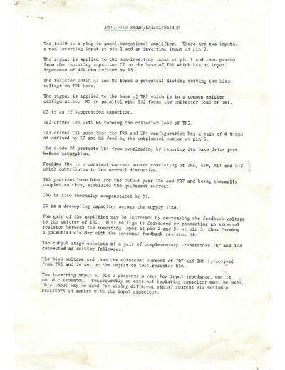
Image preview - the first page of the document

>> Download 0440_BA440_class_AB_line_amplifier_doc_4pages documenatation <<
Text preview - extract from the document
                       AMPLIFIER BA440/BA440A/BA440B


The BA440 is a plug in quasi-operational amplifier. There are two inputs,
a non inverting input at pin 1 and an inverting input at pin 2.

The signal is applied to the non-inverting input at pin 1 and then passes
from the isolating capacitor C2 to the base of TR1 which has an input
impedance of 47K ohm defined by R3.

The resistor chain Rl and R2 forms a potential divider setting the bias
voltage on TR1 base.

The signal is applied to the base of TR2 which is in a common emitter
configuration. R5 in parallel with TR2 forms the collector load of TR1.

C3 is an rf suppression capacitor.

TR2 drives TR3 with R6 forming the collector load of TR2.

TR3 drives TR4 such that the TR3 and TR4 configuration has a gain of 4 times
as defined by R7 and R8 feeding the unbalanced output at pin 5.

The diode D3 protects TR4 from overloading by removing its base drive just
before saturation.

Feeding TR4 is a constant current source consisting of TR6, RIO, Rll and R12
which contributes to low overall distortion.

TR5 provides base bias for the output pair TR6 and TR7 and being thermally
coupled to them, stabilies the quiescent current.

TR6 is also thermally compenstated by Dl.

C5 is a decoupling capacitor across the supply line.

The gain of the amplifier may be increased by decreasing the feedback voltage
to the emitter of TR1. This voltage is decreased by connecting an external
resistor between the inverting input at pin 2 and B- at pin 3, thus forming
a potential divider with the internal feedback resistor R4.

The output stage consists of a pair of complementary transistors TR7 and TR8
connected as emitter followers.

The bias voltage and thus the quiescent current of TR7 and TR8 is derived
from TR5 and is set by the adjust on test,resistor R16.
                                        '-
The inverting input at pin 2 presents a very low input impedance, but is
not d.c isolated. Consequently an external isolating capacitor must be used
This input may be used for mixing different signal sources via suitable
resistors in series with the input capacitor.
◦ Jabse Service Manual Search 2024 ◦ Jabse Pravopis ◦ onTap.bg ◦ Other service manual resources online : Fixya ◦ eServiceinfo