Service Manuals, User Guides, Schematic Diagrams or docs for : Marantz CR CR-710 CR-710

<< Back | Home

Most service manuals and schematics are PDF files, so You will need Adobre Acrobat Reader to view : Acrobat Download Some of the files are DjVu format. Readers and resources available here : DjVu Resources
For the compressed files, most common are zip and rar. Please, extract files with Your favorite compression software ( WinZip, WinRAR ... ) before viewing. If a document has multiple parts, You should download all, before extracting.
Good luck. Repair on Your own risk. Make sure You know what You are doing.


Image preview - the first page of the document
CR-710


>> Download CR-710 documenatation <<

Text preview - extract from the document
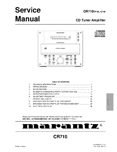
Service                                                                                                                                                             CR710/F1W, /C1W

Manual                                                                                                                                                CD Tuner Amplifier


                                                                                                                                                           DISC 1


                                                                                                                                                           DISC 2
                                                                         1
                                                                         2
                                                                         3


                                                                                                                                                           DISC 3


                                                                                          CD TUNER AMPLIFIER CR710


                                                                                         3 CD MULTI CHANGER


                                                POWER          CD /           TUNER /                                  TUNING / PRESET / TIME    PLAY /
                                              STANDBY / ON   MD / TAPE         AUX                VOLUME                                         BAND


                                                                              TUNING                                  PROGRAM /                  PAUSE /
                                                              TIMER            MODE                                  MEMORY / SET   DISC SKIP   FM MODE


                                                             PHONES                                                                              STOP /
                                                                             TIME MODE                                JOG MODE         EQ        CLEAR

                                                                                           DOWN              UP


                                                                             TABLE OF CONTENTS
                    1.    TECHNICAL SPECIFICATIONS ............................................................................. 1
                    2.    WIRING DIAGRAM ................................................................................................. 2
                    3.    BLODK DIAGRAM .................................................................................................. 3
                    4.    SCHEMATIC DIAGRAM AND PARTS LOCATION (Parts side) .............................. 5
                    5.    MICROPROCESSOR AND IC DATA .................................................................... 13
                    6.    ADJUSTMENT PROCEDURE .............................................................................. 20
                    7.    REMOVE DISC HOW-TO ..................................................................................... 22


                                                                                                                                                                                                CR710
                    8.    EXPLODED VIEW AND PARTS LIST FOR CABINET ......................................... 23
                    9.    EXPLODED VIEW AND PARTS LIST FOR MECHANISM ASS'Y ........................ 26
                    10.   ELECTRICAL PARTS LIST ................................................................................... 28


           Please use this service manual with referring to the user guide (D.F.U) without fail.


                                                                                CR710
                                                                                                                                                                          307W855010 AO
Printed in Japan                                                                                                                                                          First Issue:2001.10
                                                    MARANTZ DESIGN AND SERVICE


Using superior design and selected high grade components, MARANTZ company has created the ultimate in stereo sound.
Only original MARANTZ parts can insure that your MARANTZ product will continue to perform to the specifications for which
it is famous.
Parts for your MARANTZ equipment are generally available to our National Marantz Subsidiary or Agent.
ORDERING PARTS :
Parts can be ordered either by mail or by Fax.. In both cases, the correct part number has to be specified.
The following information must be supplied to eliminate delays in processing your order :
1. Complete address
2. Complete part numbers and quantities required
3. Description of parts
4. Model number for which part is required
5. Way of shipment
6. Signature : any order form or Fax. must be signed, otherwise such part order will be considered as null and void.


  USA                                            EUROPE / TRADING                           BRAZIL
 MARANTZ AMERICA, INC.   INC                     MARANTZ EUROPE B.V.                       PHILIPS DA AMAZONIA IND. ELET. ITDA
 1100 MAPLEWOOD DRIVE                            P.O.BOX 80002, BUILDING SFF2              CENTRO DE INFORMACOES AO
 ITASCA, IL. 60143                               5600 JB EINDHOVEN                         CEP 04698-970
 USA                                             THE NETHERLANDS                           SAO PAULO, SP, BRAZIL
 PHONE : 630 - 741 - 0300                        PHONE : +31 - 40 - 2732241                PHONE : 0800 - 123123(Discagem Direta Gratuita)
 FAX    : 630 - 741 - 0301                       FAX     : +31 - 40 - 2735578              FAX    : +55 11 534. 8988


                           AMERICAS                                    AUSTRALIA            CANADA
 SUPERSCOPE TECHNOLOGIES, INC.                  TECHNICAL AUDIO GROUP PTY, LTD             LENBROOK INDUSTRIES LIMITED
 MARANTZ PROFESSIONAL PRODUCTS                  558 DARLING STREET,                        633 GRANITE COURT,
 2640 WHITE OAK CIRCLE, SUITE A                 BALMAIN, NSW 2041,                         PICKERING, ONTARIO L1W 3K1
 AURORA, ILLINOIS 60504 USA                     AUSTRALIA                                  CANADA
 PHONE : 630 - 820 - 4800                       PHONE : 61 - 2 - 9810 - 5300               PHONE : 905 - 831 - 6333
 FAX    : 630 - 820 - 8103                      FAX    : 61 - 2 - 9810 - 5355              FAX    : 905 - 831 - 6936


   AUSTRALIA                                     THAILAND                                   SINGAPORE
 QualiFi Pty Ltd,                               MRZ STANDARD CO.,LTD                       WO KEE HONG DISTRIBUTION PTE LTD
 24 LIONEL ROAD,                                746 - 754 MAHACHAI ROAD.,                  130 JOO SENG ROAD
 MT. WAVERLEY VIC 3149                          WANGBURAPAPIROM, PHRANAKORN,               #03-02 OLIVINE BUILDING
 AUSTRALIA                                      BANGKOK, 10200 THAILAND                    SINGAPORE 368357
 PHONE : +61 - (0)3 - 9543 - 1522               PHONE : +66 - 2 - 222 9181                 PHONE : +65 858 5535 / +65 381 8621
 FAX     : +61 - (0)3 - 9543 - 3677             FAX     : +66 - 2 - 224 6795               FAX     : +65 858 6078


   NEW ZEALAND                                   TAIWAN                                     MALAYSIA
 WILDASH AUDIO SYSTEMS NZ                       PAI- YUING CO., LTD.                       WO KEE HONG ELECTRONICS SDN. BHD.
 14 MALVERN ROAD MT ALBERT                      6 TH FL NO, 148 SUNG KIANG ROAD,           SUITE 8.1, LEVEL 8, MENARA GENESIS,
 AUCKLAND NEW ZEALAND                           TAIPEI, 10429, TAIWAN R.O.C.               NO. 33, JALAN SULTAN ISMAIL,
 PHONE : +64 - 9 - 8451958                      PHONE : +886 - 2 - 25221304                50250 KUALA LUMPUR, MALAYSIA
 FAX    : +64 - 9 - 8463554                     FAX     : +886 - 2 - 25630415              PHONE : +60 3 - 2457677
                                                                                           FAX     : +60 3 - 2458180


  JAPAN Technical                                                                           KOREA
 MARANTZ JAPAN, INC.                                                                       MK ENTERPRISES LTD.
 35- 1, 7- CHOME, SAGAMIONO                                                                ROOM 604/605, ELECTRO-OFFICETEL, 16-58,
 SAGAMIHARA - SHI, KANAGAWA                                                                3GA, HANGANG-RO, YONGSAN-KU, SEOUL
 JAPAN 228-8505                                                                            KOREA
 PHONE : +81 42 748 1013                                                                   PHONE : +822 - 3232 - 155
 FAX       : +81 42 741 9190                                                               FAX    : +822 - 3232 - 154


SHOCK, FIRE HAZARD SERVICE TEST :
CAUTION : After servicing this appliance and prior to returning to customer, measure the resistance between either primary AC
cord connector pins ( with unit NOT connected to AC mains and its Power switch ON ), and the face or Front Panel of product and
controls and chassis bottom.
Any resistance measurement less than 1 Megohms should cause unit to be repaired or corrected before AC power is applied, and
verified before it is return to the user/customer.
Ref. UL Standard No. 1492.


                                      In case of difficulties, do not hesitate to contact the Technical
                                      Department at above mentioned address.
                                                                                                                                       010620 A.O
1. TECHNICAL SPECIFICATIONS

Amplifier section
1 kHz con tinuou s outpu ........... stereo chann el drive,
                                                      2ch x 20W, 0.5%
S/N ................................. Aux, Tape, MD (IHF-A) 90dB
Inpu t sensitivity & Impedance ... Aux, Tape, MD(IHF-A)
                                                                       200mV
Frequ ency character Aux, Tape, MD 10Hz 60kHz (-3dB)
Ton e control: Treble ............................................ 9dB
                     Bass .............................................. 9dB

Tuner section

Frequ ency range... 87.5 108.00 MHz (100kHz interval)
Inpu t Sensitivity................................. 15dB (S/N 30dB)
To tal Harmonic Distortion .................................... 0.2%
S/N ratio: Mono .................................................... 65dB
           Stereo .................................................. 60dB
Stereo separation 1kHz ....................................... 35dB


Frequ ency range ........... 522 1620 kHz (9kHz interval)
Inpu t sensitivity ................................. 50dB (S/N 20dB)
To tal Harmonic Distortion .................................... 1.5%
S/N ratio ............................................................... 40dB


CD section
Chann els .................................................... 2 Chann els
Frequ ency respon se .............. 20Hz 20,000Hz 1.5dB
S/N ratio ..................................... 87dB (IHF `A' Fil ter)
Distortion ........................................................... 0.1%
Chann el separation ................................ 65dB (1kHz)
Sampli ng rate ................................................. 44.1kHz
Err or corr ection ................................................... CIRC
D/A con version..CMOS delta-Sigma D/A con verter(1 Bit)
Optical readou t
Laser ........................................... Semicondu ctor laser
Wave leng th ........................................................ 780nm

General
Power supp ly .............................................. 220V, 60Hz
Power con sumption ............................................ 105W
Dimension (W x H x D) ..................175 x 140 x 360 mm
Weigh t ................................................................. 4.0kg


                                                                                  1
2. WIRING DIAGRAM


                    2
3. BLOCK DIAGRAM


                   3   4
4. SCHEMATIC DIAGRAM AND PARTS LOCATION (Parts side)


                                      5                6
                                                                                         Q905   Q906
           Q701   Q306 Q307                                                              Q369   Q904   Q903
           IC25   Q207 Q305 Q911 Q918                           Q362               IC91  Q368   Q370    IC21                             Q202                             Q506
MAIN PCB   Q205   Q206 Q208 Q920 Q917   IC36        IC37   Q363 Q361 Q212 Q915 Q916 Q901 Q211   Q213 Q902 IC22                      Q201 Q203 Q204      Q504 Q503    Q507 Q505 Q502          IC52


                                                                                                                                                                                                    Q909


                                                                                                                                                                                                    Q908


                                                                                                   IC13          Q109   Q104 Q107 Q103   Q108    IC12               IC11              Q101
                                    INPUT PCB                                       TUNER PCB                              Q110
  SPK TERMINAL PCB


                                                7                                                                                                                          8
9   10
FRONT PCB                                 CD MECHANISM PCB


                                   Q603

                                   Q602


                                   IC64
                                   IC66                        IC66
                                   IC65


                            Q701


                                   IC62            IC62


                                   Q601

                                   IC63


                                   IC61


            HEADPHONE PCB


            11                                            12
  5. MICROPROCESSOR AND IC DATA
IC36 : BVIANAM1301T                                                                                                                                                                              IC66 : BVIANAM1325AC
PIN CONFIGURATION                                                                                    PIN FUNCTION                                                                                PIN CONFIGURATION                                                                                   PIN FUNCTION


                                                                                                                                                                                                                       (S29) PD7
                                                                                                                                                                                                                       (S28) PD6
                                                                                                                                                                                                                       (S27) PD5
                                                                                                                                                                                                                       (S26) PD4
                                                                                                                                                                                                                       (S25) PD3
                                                                                                                                                                                                                       (S24) PD2
                                                                                                                                                                                                                       (S23) PD1
                                                                                                                                                                                                                       (S22) PD0
                                                                                                                                                                                                                       (S38) PE0
                                                                                                                                                                                                                       (S37) PE7
                                                                                                                                                                                                                       (S36) PE6
                                                                                                                                                                                                                       (S35) PE5
                                                                                                                                                                                                                       (S34) PE4
                                                                                                                                                                                                                       (S33) PE3
                                                                                                                                                                                                                       (S32) PE2
                                                                                                                                                                                                                       (S31) PE1
                                                                                                                                                                                                                       (S30) PE0
                                                                                                                                                                                                                       (S39) PF1
                      (S29) PD7
                      (S28) PD6
                      (S27) PD5
                      (S26) PD4
                      (S25) PD3
                      (S24) PD2
                      (S23) PD1
                      (S22) PD0


                                                                                                                                                                                                                       (S21) P97
                                                                                                                                                                                                                       (S20) P96
                      (S38) PE0
                      (S37) PE7
                      (S36) PE6
                      (S35) PE5
                      (S34) PE4
                      (S33) PE3
                      (S32) PE2
                      (S31) PE1
                      (S30) PE0
                      (S39) PF1


                      (S21) P97
                      (S20) P96
                                                                                                      PIN No.          NAME              I/ O                          DESCRIPTION                                                                                                                    PIN No.            NAME             I/ O                          DESCRIPTION
                                                                                                          1, 25            VDD            -      POWER SUPPLY (+5V)                                                                                                                                       1, 25            VDD             -      POWER SUPPLY (+5V)
                                                                                                           6              HREQ           I/O     BUS for CD CLOCK                                                                                                                                          2             BUS 0            I/O     BUS for CD DATA
                                                                                                           7           SLQCLK            I/O     BUS for CD CHIP ENABLE                                                                                                                                    3             BUS 1            I/O     BUS for CD DATA
                                                                                                           8            SLQIN             I      RESET for CD                                                                                                                                              4             BUS 2            I/O     BUS for CD DATA
                                                                                                           9           SLQOUT             O      MUTE for CD SINGLE                                                                                                                                        5             BUS 3            I/O     BUS for CD DATA
                                                                                                           12             DATA            O                                                                                                                                                                6               BUCK           I/O     BUS for CD CLOCK


                                                                                                                                                                                                                       100
                                                                                                                                                                                                                       99
                                                                                                                                                                                                                       98
                                                                                                                                                                                                                       97
                                                                                                                                                                                                                       96
                                                                                                                                                                                                                       95
                                                                                                                                                                                                                       94
                                                                                                                                                                                                                       93
                                                                                                                                                                                                                       92
                                                                                                                                                                                                                       91
                                                                                                                                                                                                                       90
                                                                                                                                                                                                                       89
                                                                                                                                                                                                                       88
                                                                                                                                                                                                                       87
                                                                                                                                                                                                                       86
                                                                                                                                                                                                                       85
                                                                                                                                                                                                                       84
                                                                                                                                                                                                                       83
                                                                                                                                                                                                                       82
                                                                                                                                                                                                                       81
                      100
                      99
                      98
                      97
                      96
                      95
                      94
                      93
                      92
                      91
                      90
                      89
                      88
                      87
                      86
                      85
                      84
                      83
                      82
                      81
                                                                                                                                                 EUROPE VERSION RDS DATA CONTROL PORT
                                                                                                           13          CLOCK              O                                                                                                                                                                7                CCE           I/O     BUS for CD CHIP ENABLE
       VDD           1                                           80             P95 (S19)                  14         STEREO IN           I      STEREO IN CONTROL INPUT
                                                                                                                                                                                                        VDD           1                                           80             P95 (S19)                 8               CDRE            O      RESET for CD
                     2                                           79             P94 (S18)                  15          TUNED              I      TUNED CONTROL INPUT
                                                                                                                                                                                                                      2                                           79             P94 (S18)                 9             MUTE              O      MUTE for CD SINGLE
                     3                                           78             P93 (S17)                  16             HPIN
                                                                                                                                                                                                                      3                                           78             P93 (S17)                 10          SIO CLOCK          I/O
                     4                                           77             P92 (S16)                  17        PROTECTOR            I      PROTECTOR IN PORT
                                                                                                                                                                                                                      4                                           77             P92 (S16)                 11           SIO OUT           I/O
                                                                                                                                                                                                                      5                                           76             P91 (S15)                                                        BUS for CD DATA
                     5                                           76             P91 (S15)            19, 20, 21      KEY MATRIX           I      KEY MATRIX PORTS                                                                                                                                          12            SIO IN           I/O
                     6                                           75             P90 (S14)             22,23,27,30          VSS            -      GND
                                                                                                                                                                                                                      6                                           75             P90 (S14)                 13              HREQ           I/O
                     7                                           74             P87 (S13)                  24          VAREF              -      A/D CONVERTOR REFERENCE VOLTAGE
                                                                                                                                                                                                                      7                                           74             P87 (S13)            22,23,27,30           VSS            -      GND
                     8                                           73             P86 (S12)                  26         BACK UP             I      BACK-UP MODE CONTROL INPUT
                                                                                                                                                                                                                      8                                           73             P86 (S12)                 31               X IN           I
                     9                                           72             P85 (S11)              28, 29             X-TAL           I      32.768kHz SUB CLOCK CONNECTING PORT
                                                                                                                                                                                                                      9                                           72             P85 (S11)                 32            X OUT             O
                                                                                                                                                                                                                                                                                                                                                  8MHz CRYSTAL CONNECTING TERMINAL
                     10                                          71             P84 (S10)                  31              X IN           I
                                                                                                                                                                                                                      10                                          71             P84 (S10)                 33            RESET             I      SYSTEM RESET
                     11                                          70             P83 (S9)                                                  O
                                                                                                                                                 8MHz CRYSTAL CONNECTING TERMINAL                                     11                                          70             P83 (S9)                  42                A             O
                                                                                                           32          X OUT
                     12                                          69             P82 (S8)                                                  I      SYSTEM RESET PULSE INPUT
                                                                                                                                                                                                                      12                                          69             P82 (S8)                  43                B             O
                                                                                                           33          RESET
                     13                                          68             P81 (S7)                                                  I      REMOTE CONTROL SIGNAL INPUT
                                                                                                                                                                                                                      13                                          68             P81 (S7)                  44                C             O
                                                                                                                                                                                                                                                                                                                                                  PLL DATA CONTROL PORT
                                                                                                           34        REMOTE IN
                     14                                          67             P80 (S6)                                                  I      REMOTE CONTROL SIGNAL INPUT
                                                                                                                                                                                                                      14                                          67             P80 (S6)                  45                D             O
                                                                                                           35          BUS IN
                     15                                          66             P77 (S5/G0)                36         BUS OUT             O      REMOTE CONTROL SIGNAL INPUT
                                                                                                                                                                                                                      15                                          66             P77 (S5/G0)               46          DSP POWER           O      CD POWER ON/OFF
                     16                                          65             P76 (S4/G1)                                                                                                                           16                                          65             P76 (S4/G1)
                                                                                                           38         SPEAKER             O      SPEAKER ON/OFFPORT                                                                                                                                        47            CD-RW             O      LOW: CD-RW, HIGH: CD
                     17                                          64             P75 (S3/G2)                                                                                                                           17                                          64             P75 (S3/G2)
                                                                                                           41              CE             O                                                                                                                                                                83        UN CLAMP SW           I
                     18                                          63             P74 (S2/G3)                                                                                                                           18                                          63             P74 (S2/G3)
                                                                                                           42         DATA OUT            O                                                                                                                                                                84        T.U HEIGHT SW         I
                     19                                          62             P73 (S1/G4)                                                      PLL DATA CONTROL PORT                                                19                                          62             P73 (S1/G4)
                                                                                                           43          CLOCK              O                                                                                                                                                                85       HOLDER MODE SW         I
                     20                                          61             P72 (S0/G5)                                                                                                                           20                                          61             P72 (S0/G5)
                                                                                                           44          DATA IN            I                                                                                                                                                                86        T.U HEIGHT SW         I
                     21                                          60             P71 (G6)                                                                                                                              21                                          60             P71 (G6)
                                                                                                           45          CLOCK              O                                                                                                                                                                87       HOLDER HEIGHT SW       I
        VSS          22                                          59             P70 (G7)                                                         TDA7318D DATA CONTROL PORT                              VSS          22                                          59             P70 (G7)                                                         MECHANISM SW CONDITION
                                                                                                           46             DATA            O                                                                                                                                                                88         LOAD/CLAMP           I
       VASS          23                                          58             P57 (G8)                                                                                                                VASS          23                                          58             P57 (G8)
                                                                                                           47          POWER              O      POWER ON/OFF                                                                                                                                              89           OPEN SW            I
     VAREF           24                                          57             P56 (G9)                                                                                                              VAREF           24                                          57             P56 (G9)
                                                                                                           48             MUTE            O      SIGNAL MUTE                                                                                                                                               90         CLOSE/HP SW          I
        VDD          25                                          56             P55 (G10)                                                                                                                VDD          25                                          56             P55 (G10)
                                                                                                           50              VFL                   (-33V) NEGATIVE POWER SUPPLY FOR FIP BLINKING                                                                                                             91         DISC ON SW           I
         P20         26                                          55             P54 (G11)                                                                                                                 P20         26                                          55             P54 (G11)
                                                                                                      52 ~ 60             GRID            O      FIP GRID CONTROL OUTPUTS                                                                                                                                  92        DISC CENTERSW         I
       TEST          27                                          54             P53 (G12)                                                                                                               TEST          27                                          54             P53 (G12)
                                                                                                      61 ~ 82         SEGMENT             O      FIP SEGMENT CONTROL OUTPUTS                       (XTIN) P21         28                                          53             P52 (G13)                100           LIMIT SW           I
  (XTIN) P21         28                                          53             P52 (G13)
                                                                                                      83 ~ 87                             I      AREA OPTION                                     (XTOUT) P22          29                                          52             P51 (G14)
(XTOUT) P22          29                                          52             P51 (G14)
                                                                                                           89         CD POWER            O      CD POWER ON/OFF PORT
        VSS          30                                          51             P50 (G15)                                                                                                                VSS          30                                          51             P50 (G15)
                                                                                                           90        ON/STBY LED          O      ON/STANDBY LED CONTROL PORT


                                                                                                                                                                                                                       31
                                                                                                                                                                                                                       32
                                                                                                                                                                                                                       33
                                                                                                                                                                                                                       34
                                                                                                                                                                                                                       35
                                                                                                                                                                                                                       36
                                                                                                                                                                                                                       37
                                                                                                                                                                                                                       38
                                                                                                                                                                                                                       39
                                                                                                                                                                                                                       40
                                                                                                                                                                                                                       41
                                                                                                                                                                                                                       42
                                                                                                                                                                                                                       43
                                                                                                                                                                                                                       44
                                                                                                                                                                                                                       45
                                                                                                                                                                                                                       46
                                                                                                                                                                                                                       47
                                                                                                                                                                                                                       48
                                                                                                                                                                                                                       49
                                                                                                                                                                                                                       50
                      31
                      32
                      33
                      34
                      35
                      36
                      37
                      38
                      39
                      40
                      41
                      42
                      43
                      44
                      45
                      46
                      47
                      48
                      49
                      50


                                                                                                           91          TAPE `H'           O      ON TAPE FUNCTION `H' OUTPUT PORT
                                                                                                           93          MD `H'             O      ON MD FUNCTION `H' OUTPUT PORT
                                                                                                       96, 97       JOG CONTROL           I      VOL/BAL/BASS/TRE CONTROL JOG INPUT PORT


                                                                                                                                                                                                                       XIN
                                                                                                                                                                                                                       XOUT
                                                                                                                                                                                                                       RESET
                                                                                                                                                                                                                       P10 (INT 0)
                                                                                                                                                                                                                       P11 (INT 1)
                                                                                                                                                                                                                       P12 (INT 2/TC 1)
                                                                                                                                                                                                                       P13 (DVO)
                                                                                                                                                                                                                       P14 (PPO)
                                                                                                                                                                                                                       P15 (TC 2)
                                                                                                                                                                                                                       P16
                                                                                                                                                                                                                       P17
                                                                                                                                                                                                                       P00
                                                                                                                                                                                                                       P01
                                                                                                                                                                                                                       P02
                                                                                                                                                                                                                       P03
                                                                                                                                                                                                                       P04
                                                                                                                                                                                                                       P05
                                                                                                                                                                                                                       P06
                                                                                                                                                                                                                       P07
                                                                                                                                                                                                                       VKK
                      XIN
                      XOUT
                      RESET
                      P10 (INT 0)
                      P11 (INT 1)
                      P12 (INT 2/TC 1)
                      P13 (DVO)
                      P14 (PPO)
                      P15 (TC 2)
                      P16
                      P17
                      P00
                      P01
                      P02
                      P03
                      P04
                      P05
                      P06
                      P07
                      VKK


BLOCK DIAGRAM                                                         OUTPUT Ports                                     I/O Ports                                                                 BLOCK DIAGRAM                                                         OUTPUT Ports                                     I/O Ports
                                  I/O Ports                                                                                                                                                                                        I/O Ports
                                     P97                              P87           P77           P57               PID7          PIE7           PIF1                                                                                 P97                              P87           P77          P57                PID7          PIE7           PIF1
                                      to                               to            to            to                to            to             to                                                                                   to                               to            to           to                 to            to             to
                                     P90                              P80           P70           P50               PID8          PIE0           PIF0                                                                                 P90                              P80           P70          P50                PID8          PIE0           PIF0

                           VDD       P9                               P8             P7              P5             PID            PIE           PIF                                                      Power Supply      VDD       P9                               P8             P7             P5              PID           PIE            PIF
         Power Supply
                           VSS                                                                                                                                                                                              VSS
                                                                                                                                                                      Key scan                                                                                                                                                                                         Key scan
         VFT Power         VKK                                         VFT drive circuit (automatic display)                                                           control                            VFT Power         VKK                                         VFT drive circuit (automatic display)                                                           control
         Supply                                                                                                                                                                                           Supply


                                                                 P S        W              Stack Pointer                  Data Memory                 Program counter                                                                                             P S        W             Stack Pointer                   Data Memory                 Program counter
                                                            Flags           RBS                                              (RAM)                                                                                                                           Flags           RBS                                              (RAM)
                                               ALU                                                                                                                                                                                              ALU
                                                                                                                                                      Program Memory                                                                                                                                                                                   Program Memory
                                                                                                                       Register banks                                                                                                                                                                                    Register banks                     (ROM)
         Reset I/O        RESET                                                                                                                            (ROM)                                          Reset I/O        RESET
                                       System Controller                                                                                                                                                                                System Controller
         Test Pin          TEST                                                                                                                                                                           Test Pin          TEST
                                                                                               Interrupt Controller                                                                                                                                                                            Interrupt Controller
                                       Standby Controller                                                                                                        Inst.                                                                  Standby Controller                                                                                                           Inst.
                                                                                                                                                                Register                                                                                                                                                                                            Register
                                                                                                                                                                 Inst.                                                                                                                                                                                               Inst.
                                       Timing Generator           Time Base                   16-bit          8-bit                         Serial              Decoder                                                                 Timing Generator           Time Base                   16-bit          8-bit                         Serial                 Decoder
                                                                    Timer                 Timer/Counters Timer/Counters                   Interfaces                                                                                                                 Timer                 Timer/Counters Timer/Counters                   Interfaces
         Resonator          XIN        High                                                                                                                                                               Resonator          XIN        High
                          XOUT        frequ.     Clock                                     TC1    TC2      TC3 TC4                       SIO HSO                                                          connecting       XOUT        frequ.     Clock                                     TC1    TC2      TC3 TC4                       SIO HSO
         connecting
         Pins                          Low      Generator         Watchdog                                                                                                                                Pins                          Low      Generator         Watchdog
                                      frequ.                       Timer                                                                                                                                                               frequ.                       Timer


                                          P2     8-bit      P6      P0                          P1                                              P3                     P4                                                                  P2     8-bit      P6      P0                         P


◦ Jabse Service Manual Search 2024 ◦ Jabse PravopisonTap.bg ◦ Other service manual resources online : FixyaeServiceinfo