Service Manuals, User Guides, Schematic Diagrams or docs for : Marantz SR SR-5000 SR-5000

<< Back | Home

Most service manuals and schematics are PDF files, so You will need Adobre Acrobat Reader to view : Acrobat Download Some of the files are DjVu format. Readers and resources available here : DjVu Resources
For the compressed files, most common are zip and rar. Please, extract files with Your favorite compression software ( WinZip, WinRAR ... ) before viewing. If a document has multiple parts, You should download all, before extracting.
Good luck. Repair on Your own risk. Make sure You know what You are doing.


Image preview - the first page of the document
SR-5000


>> Download SR-5000 documenatation <<

Text preview - extract from the document
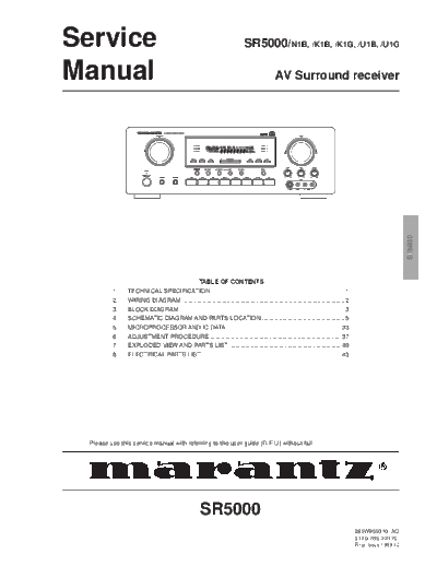
Service                                                                    SR5000/N1B, /K1B, /K1G, /U1B, /U1G

Manual                                                                                     AV Surround receiver


                                                                                                                                                           SR5000
                                                    TABLE OF CONTENTS
          1.    TECHNICAL SPECIFICATION ............................................................................... 1
          2.    WIRING DIAGRAM ................................................................................................. 2
          3.    BLOCK DIAGRAM .................................................................................................. 3
          4.    SCHEMATIC DIAGRAM AND PARTS LOCATION ................................................. 5
          5.    MICROPROCESSOR AND IC DATA .................................................................... 33
          6.    ADJUSTMENT PROCEDURE .............................................................................. 37
          7.    EXPLODED VIEW AND PARTS LIST ................................................................... 40
          8.    ELECTRICAL PARTS LIST ................................................................................... 43


  Please use this service manual with referring to the user guide (D.F.U) without fail.


                                                     SR5000
                                                                                                                                     285W855010 AO
                                                                                                                                     3120 785 22170
                                                                                                                                     First Issue:1999.10
                                                 MARANTZ DESIGN AND SERVICE


Using superior design and selected high grade components, MARANTZ company has created the ultimate in stereo sound.
Only original MARANTZ parts can insure that your MARANTZ product will continue to perform to the specifications for which
it is famous.
Parts for your MARANTZ equipment are generally available to our National Marantz Subsidiary or Agent.
ORDERING PARTS :
Parts can be ordered either by mail or by Fax.. In both cases, the correct part number has to be specified.
The following information must be supplied to eliminate delays in processing your order :
1. Complete address
2. Complete part numbers and quantities required
3. Description of parts
4. Model number for which part is required
5. Way of shipment
6. Signature : any order form or Fax. must be signed, otherwise such part order will be considered as null and void.


  USA                                         EUROPE / TRADING                           BRAZIL
 MARANTZ AMERICA, INC    INC.                 MARANTZ EUROPE B.V.                       MARANTZ BRAZIL
 440 MEDINAH ROAD                             P.O.BOX 80002, BUILDING SFF2              CAIXA POSTAL 21462
 ROSELLE, ILLINOIS 60172                      5600 JB EINDHOVEN                         CEP 04698-970
 USA                                          THE NETHERLANDS                           SAO PAULO, SP, BRAZIL
 PHONE : 630 - 307 - 3100                     PHONE : +31 - 40 - 2732241                PHONE : 0800 - 123123(Discagem Direta Gratuita)
 FAX    : 630 - 307 - 2687                    FAX     : +31 - 40 - 2735578              FAX    : +55 11 534. 8988


                          AMERICAS             CANADA
 SUPERSCOPE TECHNOLOGIES, INC.                LENBROOK INDUSTRIES LIMITED
 MARANTZ PROFESSIONAL PRODUCTS                633 GRANITE COURT,
 2640 WHITE OAK CIRCLE, SUITE A               PICKERING, ONTARIO L1W 3K1
 AURORA, ILLINOIS 60504 USA                   CANADA
 PHONE : 630 - 820 - 4800                     PHONE : 905 - 831 - 6333
 FAX    : 630 - 820 - 8103                    FAX    : 905 - 831 - 6936


   AUSTRALIA                                   THAILAND                                  SINGAPORE
  JAMO AUSTRALIA PTY LTD                     MRZ STANDARD CO.,LTD                        WO KEE HONG (S) PTE LTD
  1 EXPO COURT, P.O. BOX 350                 746 - 754 MAHACHAI ROAD.,                   WO KEE HONG CENTRE
  MT. WAVERLEY VIC 3149                      WANGBURAPAPIROM, PHRANAKORN,                NO.23, LORONG 8, TOA PAYOH
  AUSTRALIA                                  BANGKOK, 10200 THAILAND                     SINGAPORE 319257
  PHONE : +61 - 3 - 9543 - 1522              PHONE : +66 - 2 - 222 9181                  PHONE : +65 2544555
  FAX    : +61 - 3 - 9543 - 3677             FAX     : +66 - 2 - 224 6795                FAX     : +65 2502213


                                              TAIWAN                                     MALAYSIA
                                             PAI- YUING CO., LTD.                        WO KEE HONG ELECTRONICS SDN. BHD.
                                             6 TH FL NO, 148 SUNG KIANG ROAD,            NO. 102 JALAN SS 21/35, DAMANSARA
                                             TAIPEI, 10429, TAIWAN R.O.C.                UTAMA, 47400 PETALING JAYA
                                             PHONE : +886 - 2 - 25221304                 SELANGOR DARUL EHSAN, MALAYSIA
                                             FAX     : +886 - 2 - 25630415               PHONE : +60 3 - 7184666
                                                                                         FAX     : +60 3 - 7173828


  JAPAN Technical                                                                        KOREA
 MARANTZ JAPAN, INC.                                                                    MK ENTERPRISES LTD.
 35- 1, 7- CHOME, SAGAMIONO                                                             ROOM 604/605, ELECTRO-OFFICETEL, 16-58,
 SAGAMIHARA - SHI, KANAGAWA                                                             3GA, HANGANG-RO, YONGSAN-KU, SEOUL
 JAPAN 228-8505                                                                         KOREA
 PHONE : +81 42 748 1013                                                                PHONE : +822 - 3232 - 155
 FAX       : +81 42 748 9190                                                            FAX    : +822 - 3232 - 154


SHOCK, FIRE HAZARD SERVICE TEST :
CAUTION : After servicing this appliance and prior to returning to customer, measure the resistance between either primary AC
cord connector pins ( with unit NOT connected to AC mains and its Power switch ON ), and the face or Front Panel of product and
controls and chassis bottom.
Any resistance measurement less than 1 Megohms should cause unit to be repaired or corrected before AC power is applied, and
verified before it is return to the user/customer.
Ref. UL Standard No. 1492.


                                   In case of difficulties, do not hesitate to contact the Technical
                                   Department at above mentioned address.
                                                                                                                                     990729A.O
1. TECHNICAL SPECIFICATIONS

FM TUNER SECTION
FREQUENCY RANGE .................................................................................................................... 87.5 - 108.0 MHz
USABLE SENSITIVITY ............................................................................................................... IHF 0.9 V/10.8 dBf


SIGNAL TO NOISE RATIO .............................................................................................. MONO/STEREO 70/65 dB
DISTORTION .................................................................................................................. MONO/STEREO 0.2/0.5 %
STEREO SEPARATION .......................................................................................................................... 1 kHz 45 dB
A.C.S ................................................................................................................................................ 400 kHz 55 dB
IMAGE REJECTION ............................................................................................................................ 98 MHz 50 dB
TUNER OUTPUT LEVEL .......................................................................... 1 kHz, 40kHz Dev 600 mV (/N1B, /K1B)
................................................................................................................................................   75 kHz (/U1B,/U1G)


AM TUNER SECTION
FREQUENCY RANGE ......................................................................................... 522 - 1620 kHz (/N1B, /K1B,/K1G)
...................................................................................................................................... 520 - 1710 kHz (/U1B,/U1G)
USABLE SENSITIVITY .................................................................................................................... LOOP 500 V/m
SIGNAL TO NOISE RATIO .......................................................................................................... 50 dB (at 94 dB/m)
DISTORTION ........................................................................................................................ 1 kHz, 30 % Mod.0.5 %
SELECTIVITY ...................................................................................................................              10 kHz 25 dB (at 85 dB)


AUDIO SECTION
RATED POWER (5ch drive)
    Front .................................................................................................................... 20 Hz - 20 kHz 8 ohms 70 W/ch
    Center .................................................................................................................................... 1 kHz 8 ohms 70 W
  Surround ........................................................................................................................... 1 kHz 8 ohms 70 W/ch
THD Front .................................................................................................................. 20 Hz - 20 kHz 8 ohms 0.09 %
INPUT SENSITIVITY/IMPEDANCE
LINEAR ......................................................................................................................................... 200 mV/47k ohms
SIGNAL TO NOISE RATIO (IHF-A)
LINEAR ............................................................................................................................................................. 92 dB


VIDEO SECTION
Input/Output Level/Impedance ....................................................................................................... 1.0 Vp-p/75 ohms


OTHERS
POWER SUPPLY ................................................................................................................... AC 230V 50 Hz (/N1B)
                                                                                                                                       AC 220V 50 Hz (/K1B,K1G)
                                                                                                                                      AC 120V 60 Hz (/U1B,/U1G)
POWER CONSUMPTION ..................................................................................................................... 380 W (/N1B)
                                                                                                                               380 W (/K1B,/K1G)
                                                                                                                                                    3.8 A (/U1B,/U1G)


DIMENSIONS (MAX)
WIDTH .......................................................................................................................................................... 440 mm
HEIGHT ......................................................................................................................................................... 153 mm
DEPTH .......................................................................................................................................................... 425 mm
WEIGHT .......................................................................................................................................................... 13.5 kg


SPECIFICATIONS SUBJECT TO CHANGE WITHOUT PRIOR NOTICE


                                                                                                    1
2. WIRING DIAGRAM


                    2
3. BLOCK DIAGRAM


                   3   4
4. SCHEMATIC DIAGRAM AND PARTS LOCATION
 Main


                                   5      6
Main Board
                                      Q955
                                      Q956                                                               Q965
          Q978   Q977   Q976   Q975   Q957                                             Q966              Q964
   Q953   Q974   Q973   Q972   Q971   Q962   IC95   IC96   IC97   IC45   IC48   IC46   Q967   IC47       Q963


                          7                                                                          8
Audio Input / Volume


                       9   10
Audio In / Volume Board


                               IC11


                               Q150, Q149


                               Q148

                               Q147


                               Q185, Q186, Q187
                               Q188, Q189, Q190


                               IC15, IC16, IC17


                               IC13


                          11
              Digital In / DSP Board


      IC35


Q302, Q301

      IC41


      IC34


      IC36


Q306, Q305
Q304, Q303


      IC42


 IC38, IC37


      IC39


      IC32


      IC31


      IC33


                                       12
Digital Input / DSP


                      13   14
Tuner (/N1)


              15   16
                Tuner Board


         Q14


          IC1


     Q12, Q11


          IC2


          IC4


         Q13


     IC3, IC5


Q16, Q15, Q17


                              17
                Tuner Board


         Q14


          IC1


     Q12, Q11


          IC2


          IC4


         Q13


     IC3, IC5


Q16, Q15, Q17


                              18
Tuner (/K1, /U1)


                   19   20
Video Input        Speaker


                   u-Com Power Supply / Standby


S-VHS Input


              21                                  22
       Video Input Board        S-VHS Input Board


                                                                          Q252, Q251


                                                                          IC25


                                                                          Q255
IC21

                                                                          Q254


                                                                          Q253


                                                                          Q903


                                                                          Q901


                                                                          Q902


          Speaker Board
                                u-Com Power Supply / Standby Board


                           23                                        24
                         S-Video
Front


                                                    Tone Control


             Power SW.
                                   Headphone
        25                                     26
                                       Q704 Q703 Q708 IC72                                                                                 Q715 Q709
                                       Q706 Q705 Q707                                                                                      Q716
Front Board                     Q718   Q710 Q711 Q712    Q713                                             IC71                             Q717


                         Power SW. Board
                         (/U1)


                         Headphone Board


       Power SW. Board
       (/N1/K1)


                                                       S-Video Board
                                                                                                                 Tone Control Board
                                                         Q281   Q282   IC28   Q293   Q291 IC27 Q292 Q278 Q277                                   IC81


                              27                                                                                                      28
Power Amp


            29   30
Power Amp Board

              Q542                                         Q545                           Q543                                   Q544                                      Q541
          Q512       Q517                               Q515    Q520                     Q513      Q518                        Q514        Q519                         Q511          Q516
    Q627 Q562               Q557    Q582 Q622    Q630    Q585    Q580 Q585 Q625     Q628 Q583      Q558 Q583 Q623          Q629 Q564       Q559 Q584 Q624        Q626    Q561          Q556    Q581 Q621
         Q647                      Q642                 Q650           Q645              Q648            Q643                 Q649              Q644                    Q646                   Q641


  Q699   Q662     Q612         Q657      Q682       Q665 Q615           Q660 Q685   Q663    Q613       Q659         Q683       Q664     Q614       Q650          Q684   Q661   Q611           Q656   Q681


                                            31                                                                                                              32
5. MICROPROCESSOR AND IC DATA
                                                                                                                                                                                                                                                                                     3. Pin Functions
IC31:YSS912


                                                                                                                                OPORT0
                                                      IPORT0
                                                                                                                                                                                                                                                                                     No.   Name        I/O    FUNCTION
                                                                                                                                                                                                                                                                                     1    VDD1          -    +5V power supply (for I/Os)
1. Block Diagram                                                                                                                                                                                                                                                                     2 RAMCEN          O     External SRAM interface /CE


                                                                                                                                                                                                                                              /CSB
                                                                                                          SCK
                                                                              /CS
                                                                                                                                                                                                                                                                                                       O


                                                                                          SO
                                                                                                                                                                                                                                                                                     3   RAMA16              External SRAM interface address 16


                                                                                               SI
                                                      7


                                                                                                                                7
                                                                                                                                                                                                                                                                                     4   RAMA15        O     External SRAM interface address 15
                                                                                                                                                                                                                                                                                     5    SDIB0        I+    PCM input 0 to Sub DSP
                                                                                                                                                                                                                                                                                     6    SDIB1        I+    PCM input 1 to Sub DSP


                                                                                                                                                                                                                                       SCK
                                                                                                                                                                                                                                                                                     7    SDIB2        I+    PCM input 2 to Sub DSP


                                                                                                                                                                                                                              SI
                                                                                                                                                                                                                                                                                     8      XI          I    Crystal oscillator connection (12.288 MHz)
                                                                                                                                                                                                                                                                                     9      XO         O     Crystal oscillator connection
                                                                                                                                                                                                                                                                                     10     VSS         -    Ground
                                                                               Microprocessor                                                                                                                               Coefficient/                                             11   AVDD          -    +3.3V power supply (for PLL circuit)
                                                                                    Interface                                                                                                                              Program RAM                                               12   SDIB3        I+    PCM input 3 to Sub DSP
                                                                                                                                                                                                                                                                                     13    TEST              Test terminal (to be open in normal use)
                          Control signals                                                                                                Control signals                                                                                                                             14    TEST              Test terminal (to be open in normal use)
                                                                                                                                                                                                                                                                                     15   OVFB         O     Detection of overflow at Sub DSP
                                                                              Control Registers                                                                                                                                                                            SDBCK1    16 DTSDATA        O     Detection of DTS data
    /SDBCK0                                                                                                                                                                                                                                                                SDWCK1    17 AC3DATA        O     Detection of AC-3 data
                                                                                                                                                                                                                                                                                     18   SDOB3        O     PCM output from Sub DSP
    SDBCK0                                                                                                                                                                                                                                                                           19    CPO         A     Output terminal for PLL, to be connected to ground through the external analog filter circuit
    SDWCK0                                                                                                                                                                                                                                                                           20    AVSS         -    Ground (or PLL circuit)
                                                                                                                                                                                                                                                                                     21   VDD2          -    +3.3V power supply (for core logic)
                                                                                                                                                                                                                                                                                     22   SDOA2        O     PCM output from Main DSP (C, LFE)
                                                                                                                                               SDOACKSEL                                         SDIBCKSEL                                             SDOBCKSEL
                                                                                                                                                                                                                                                                                     23   SDOA1        O     PCM output from Main DSP (LS, RS)
                                                                                                                                                                                                                                                                                     24   SDOA0        O     PCM output from Main DSP (L, R)
                                                                                                                                                                    L, R                                                                                                             25 RAMA14         O     External SRAM interface address 14
                                                                                                           AC-3/Pro Logic/DTS


                                                                                                                                                                                                                                                          SDOB Interface
                                                                                                                                                                                                                                                                                                       O


                                                                                                                                                   SDOA Interface
                                                                                                                                                                                                                                                                                     26 RAMA13               External SRAM interface address 13
                              SDIA Interface


                                                                                                                                                                                                                                                                           SDOB0


                                                                                                                                                                                                    SDIB Interface
                                                                                                                                                                                       SDIBSEL
                                                                                                                                                                                                                                                                                     27 RAMA12         O     External SRAM interface address 12
                                                               Input Buffer


                                                                                                                                                                      LS, RS
                                                                                                                                Main DSP
                SDIASEL


                                                                                                decoder


                                                                                                                                                                                                                                   Sub DSP
      SDIA0                                                                                                                                                                                                                                                                          28 RAMA11         O     External SRAM interface address 11
                                                                                                                                 24 * 24


                                                                                                                                                                                                                                    24 * 16
                                                                                                                                                                                                                                                                           SDOB1
                                                                                                                                                                                                                                                                                     29 RAMA10         O     External SRAM interface address 10
                                                                                                                                                                           C, LFE                                                                                                    30     VSS         -    Ground
      SDIA1                                                                                                                                                                                                                                                                SDOB2     31   VDD1          -    +5V power supply (for I/Os)
                                                                                                                                                                                                                                                                                     32 OPORT0         O     Output port for general purpose
                                                                                                                                                                                                                                                                           SDOB3     33 OPORT1         O     Output port for general purpose
                                                                                                                                                                                                                                                                                     34 OPORT2         O     Output port for general purpose
                                                                                                                                                                                                                                                                                     35 OPORT3         O     Output port for general purpose
                                                                                                                                                                                                                                                                                     36 OPORT4         O     Output port for general purpose
    SURENC                                     STREAM0                              7                                                                                                                                                                                                37 OPORT5         O     Output port for general purpose
   KARAOKE                                                                                                                                                                                                           External RAM                                                    38 OPORT6         O     Output port for general purpose
      MUTE                                      Operating clock                                                                                                                                                       interface                                                      39 OPORT7         O     Output port for general purpose
                               CRC


       CRC                                                                (30MHz)                                                                                                                                                                    Data RAM                        40     VSS         -    Ground
   AC3DATA                                                                                                                                                                             ERAMUSE                                                                                       41   VDD2          -    +3.3V power supply (for core logic)
                                                                                                          Delay RAM                                                                                                                                                                  42  RAMA9         O     External SRAM interface address 9
   DTSDATA                                                 PLL                                                                                                                                                                                                                       43  RAMA8         O     External SRAM interface address 8
    NONPCM                                                                                                                                                                                                                                                                                             O
                                                                                                                                                                                                                                                                                     44  RAMA7               External SRAM interface address 7
                                                                                                                                                                                                                                                                                     45   SDOB2        O     PCM output from Sub DSP
                                                                                                                                                                                                                                                                                     46   SDOB1        O     PCM output from Sub DSP
                                                 XI

                                                           XO

                                                                                    CPO


                                                                                                                                                                    SDOA0
                                                                                                                                                                    SDOA1
                                                                                                                                                                    SDOA2

                                                                                                                                                                               SDIB0
                                                                                                                                                                               SDIB1
                                                                                                                                                                               SDIB2
                                                                                                                                                                               SDIB3


                                                                                                                                                                                                     RAMD0 7

                                                                                                                                                                                                                        RAMCEN
                                                                                                                                                                                                                        RAMWEN
                                                                                                                                                                                                                        RAMOEN
                                                                                                                                                                                                                        RAMA0 16
                                                                                                                                                                                                                        OVFB
                                                                                                                                                                                                                                                                                     47   SDOB0        O     PCM output from Sub DSP
                                                                                                                                                                                                                                                                                     48 SDBCK1         I+    Bit clock input for SDOA, SDIB, SDOB
                                                                                                                                                                                                                                                                                     49 SDWCK1         I+    Word clock input for SDOA, SDIB, SDOB
                                                                                                                                                                                                                                                                                     50     VSS         -    Ground
                                                                                                                                                                                                                                                                                     51   VDD2          -    +3.3V power supply (for core logic)
                                                                                                                                                                                                                                                                                     52 NONPCM         O     Detection of non-PCM data
                                                                                                                                                                                                                                                                                     53    CRC         O     Detection of AC-3 CRC error
2. Pin Configuration                                                                                                                                                                                                                                                                 54   MUTE
                                                                                                                                                                                                                                                                                     55 KARAOKE
                                                                                                                                                                                                                                                                                                       O
                                                                                                                                                                                                                                                                                                       O
                                                                                                                                                                                                                                                                                                             Detection of auto mute
                                                                                                                                                                                                                                                                                                             Detection of AC-3 karaoke data
                                        DTSDATA
                                        AC3DATA


                                        RAMCEN


                                                                                                                                                                                                                                                                                     56 SURENC                Detection of AC-3 2/0 mode Dolby surround encoded input
                                         RAMA15


                                                                                                                                                                                                                                                                                                       O
                                         RAMA12
                                         RAMA10
                                         RAMA11

                                         RAMA13
                                         RAMA14


                                         RAMA16
                                          SDOA2


                                          SDOB3
                                          SDOA0
                                          SDOA1


                                                                                                                                                                                                                                                                                     57 /SDBCK0        O      Inverted SDBCK0 colck output (refer to Block diagram)
                                           SDIB2

                                           SDIB0
                                           SDIB3


                                           SDIB1
                                           AVDD
                                           VDD2


                                           VDD1
                                           OVFB
                                            AVSS


                                            TEST
                                            TEST


                                                                                                                                                                                                                                                                                     58  RAMA6         O      External SRAM interface address 6
                                             CPO
                                             VSS


                                             VSS
                                              XO


                                                                                                                                                                                                                                                                                     59  RAMA5         O      External SRAM interface address 5
                                               XI


                                                                                                                                                                                                                                                                                     60     VSS         -     Ground
                                                                                                                                                                                                                                                                                     61  RAMA4         O      External SRAM interface address 4
                                                                                                                                                                                                                                                                                     62     /IC        Is     Initial clear
                                                                                                                                                                                                                                                                                     63   TEST                Test terminal (to be open in normal use)
                                                                                                                                                                                                                                                                                     64  RAMA3          O     External SRAM interface address 3
                                         30


                                         26


                                         23


                                         20

                                         18

                                         16
                                         15
                                         14
                                         13
                                         12

                                         10


                                         1
                                         29
                                         28
                                         27

                                         25
                                         24

                                         22
                                         21

                                         19

                                         17


                                         11


                                         8
                                         7
                                         6
                                         5
                                         4
                                         3
                                         2
                                         9


                                                                                                                                                                                                                                                                                     65    /CSB        Is+    Sub DSP Chip select
         VDD1                 31                                                                                                                                                                                                                                                     66     /CS         Is    Microprocessor interface Chip select input
                                                                                                                                                                                                                                100                     VSS                          67     SO          Ot    Microprocessor interface Serial data output
       OPORT0                 32                                                                                                                                                                                                 99                     IPORT0                       68      SI         Is    Microprocessor interface / Sub DSP Serial data input
       OPORT1                 33                                                                                                                                                                                                                                                     69    SCK          Is    Microprocessor interface / Sub DSP clock input
                                                                                                                                                                                                                                 98                     IPORT1                       70  RAMA2          O     External SRAM interface address 2
       OPORT2                 34                                                                                                                                                                                                 97                     IPORT2                       71   VDD1           -    +5V power supply (for I/Os)
       OPORT3                 35                                                                                                                                                                                                 96                     IPORT3                       72  RAMD0        I+/O    External SRAM interface data (STREAM0 output when External   SRAM   is   not   in   use)
                                                                                                                                                                                                                                                                                     73  RAMD1        I+/O    External SRAM interface data (STREAM1 output when External   SRAM   is   not   in   use)
       OPORT4                 36                                                                                                                                                                                                 95                     IPORT4                       74  RAMD2        I+/O    External SRAM interface data (STREAM2 output when External   SRAM   is   not   in   use)
       OPORT5                 37                                                                                                                                                                                                 94                     IPORT5                       75  RAMD3        I+/O    External SRAM interface data (STREAM3 output when External   SRAM   is   not   in   use)
                                                                                                                                                                                                                                                                                     76  RAMD4        I+/O    External SRAM interface data (STREAM4 output when External   SRAM   is   not   in   use)
       OPORT6                 38                                                                                                                                                                                                 93                     IPORT6                       77  RAMD5        I+/O    External SRAM interface data (STREAM5 output when External   SRAM   is   not   in   use)
       OPORT7                 39                                                                                                                                                                                                 92                     IPORT7                       78  RAMD6        I+/O    External SRAM interface data (STREAM6 output when External   SRAM   is   not   in   use)
                                                                                                                                                                                                                                                                                     79  RAMD7        I+/O    External SRAM interface data (STREAM7 output when External   SRAM   is   not   in   use)
          VSS                 40                                                                                                                                                                                                 91                     VDD2                         80     VSS          -    Ground
         VDD2                 41                                                                                                                                                                                                 90                     VSS                          81   VDD2           -    +3.3V power supply (for core logic)
       RAMA9                  42                                                                                                                                                                                                                                                     82 SDWCK0           I    Word clock input for SDIA, SDOA, SDIB, SDOB
                                                                                                                                                                                                                                 89                     RAMOEN                       83 SDBCK0           I    Bit clock input for SDIA, SDOA, SDIB, SDOB
       RAMA8                  43                                                                                                                                                                                                 88                     RAMWEN                       84   SDIA0          I    AC-3 bitstream (or PCM) data input for Main DSP
       RAMA7                  44                                                                                                                                                                                                 87                     RAMA0                        85   SDIA1          I    AC-3 bitstream (or PCM) data input for Main DSP
                                                                                                                                                                                                                                                                                     86  RAMA1          O     External SRAM interface address 1
        SDOB2                 45                                                                                                                                                                                                 86                     RAMA1                        87  RAMA0          O     External SRAM interface address 0
        SDOB1                 46                                                                                                                                                                                                 85                     SDIA1                        88 RAMWEN          O     External SRAM interface /WE
                                                                                                                                                                                                                                                                                     89 RAMOEN          O     External SRAM interface /OE
        SDOB0                 47                                                                                                                                                                                                 84                     SDIA0                        90     VSS          -    Ground
      SDBCK1                  48                                                                                                                                                                                                 83                     SDBCK0                       91   VDD2           -    +3.3V power supply (for core logic)
                                                                                                                                                                                                                                                                                     92  IPORT7         I+    Input port for general purpose
      SDWCK1                  49                                                                                                                                                                                                 82                     SDWCK0                       93  IPORT6         I+    Input port for general purpose
          VSS                 50                                                                                                                                                                                                 81                     VDD2                         94  IPORT5         I+    Input port for general purpose
                                               52
                                               53
                                               54
                                               55
                                               56
                                               57
                                               58
                                               59
                                               60


                                               66
                                               67


                                               71


                                               74
                                               75
                                               76


                                               79
                                               51


                                               62
                                               63

                                               65


                                               69


                                               73


                                               77
                                               78

                                               80
                                               61


                                               64


                                               68

                                               70

                                               72


                                                                                                                                                                                                                                                                                     95  IPORT4         I+    Input port for general purpose
                                                                                                                                                                                                                                                                                     96  IPORT3         I+    Input port for general purpose


◦ Jabse Service Manual Search 2024 ◦ Jabse PravopisonTap.bg ◦ Other service manual resources online : FixyaeServiceinfo