Service Manuals, User Guides, Schematic Diagrams or docs for : ALPINE Car Audio PKG-2100P TMX-R2100P Alpine_PKG-2100P_TMX-R2100P

<< Back | Home

Most service manuals and schematics are PDF files, so You will need Adobre Acrobat Reader to view : Acrobat Download Some of the files are DjVu format. Readers and resources available here : DjVu Resources
For the compressed files, most common are zip and rar. Please, extract files with Your favorite compression software ( WinZip, WinRAR ... ) before viewing. If a document has multiple parts, You should download all, before extracting.
Good luck. Repair on Your own risk. Make sure You know what You are doing.


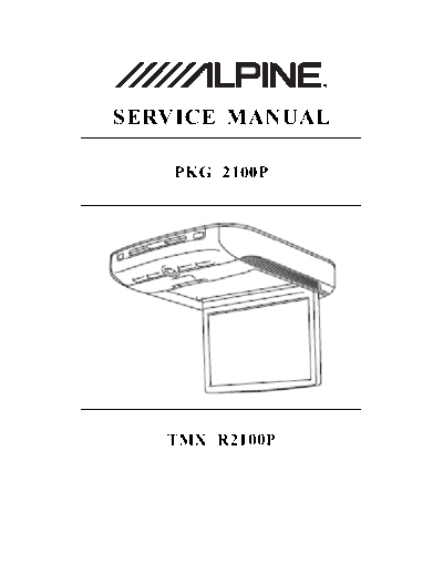
Image preview - the first page of the document
Alpine_PKG-2100P_TMX-R2100P


>> Download Alpine_PKG-2100P_TMX-R2100P documenatation <<

Text preview - extract from the document
R
                                   Contents

1.  Feature                                                             3
2.  System Connector                                                    4
3.  TMX-2100P Adjust Procedures                                        5
4.  Block Diagram                                                      6
5.  Description and Voltage of IC Terminial                        7 ~ 21
6.  Electronic Parts List                                         22 ~35
7.  Mechanical Parts List                                         36 ~37
8.  Schematic
    1) Main Board                                                 38 ~ 45
    2) TFT Board                                                  46 ~ 49
    3) FrontKeyBoard                                              50 ~ 51
    4) FrontPassengerBoard                                            52
    5) FMSwitchBoard                                                  53
    6) EjectKeyBoard                                                  54
    7) Aux3Board                                                      55
9. PCB Layout                                                      56~69
10. Connecting Table                                                  70
11. Exploded of Packaging Drawing                                     71
12. Exploded of Cabinet Drawing                                       72
13. Exploded Drawing
    a. Exploded Drawing 1~2                                            73
    b. Exploded Drawing 3~6                                            74
    c. Exploded Drawing 7~9                                            75
    d. Exploded Drawing 10~12                                          76
14. Appendix (DV39M020)                                          77 ~ 103


NOTE : Due to continuing product improvement,specifications and designs are
       subject to change without notice


                                                                              2
                                Features
1. 10.2 inch Wide VGA TFT Active Matrix Color LCD (800 x 480)
2. 2AUX In ( AUX1:AV or S-Video, AUX2:AV) /1 AUX Out
3. 1 Remote In / 2 Remote Out
4. Built-in DVD Player
5. DVB-T(EU) / ISDB-T(JP) Digital TV Ready
6. 2ch Selectable IR Transmitter ( A/ B/ Off )
7. Wired FM Modulator ( U.S.A. / JPN / EUR )
8. Auto Audio Level Control
9. Customized Opening and Wallpaper
10. DISC IN Indicator
11. White LED Dome Light
12. Customized OSD Source Name
13. Visual EQ
14. Picture Control (Bright /Color /Tint /Contrast /Sharp)
15. Auto Dimmer Control ( HIGH / LOW/AUTO)
16. Screen Mode (WIDE / CINEMA / NORMAL)
17. ISP Software Update Function


                                                                3
System Connections


                     PKG-2100P DVD Built-In
                       Overhead Monitor


                        When the game port and
                        AUX2 are connected at the
                        same time, the game port has
                        a priority.


                                                       4
Adjustment Procedures
Equipment
1                      Digital OscilloScope (For frequency measurements)
2                      Wireless Headphone
3                      Multi-meter Fluke F17B or equivalent
4                      Adjustment Tool (Small non-metallic screwdriver or equivalent)
5                      Testing Fixture (To hold Monitor in place)
6                      Power Supply ( 12VDC)


A. IR Transmitter Adjust (FrontKey Board):
Step         Measure     Adjust      Value              Description            Apparatus
                                               1)   SELECT A_CH
    1    U1 PIN8          VR3       2.8MHz     2)   Touch U1 PIN 8, Adjust   OscilloScope
                                                    VR3
                                               1)   SELECT A_CH
    2    U1 PIN12         VR1      2.3 MHz     2)   Touch U1 PIN 12,         OscilloScope
                                                    Adjust VR1
                                               1)   SELECT B_CH
    3    U1 PIN8          VR4      3.8 MHz     2)   Touch U1 PIN 8, Adjust   OscilloScope
                                                    VR4
                                               1)   SELECT B_CH
    4    U1 PIN12         VR2      3.2 MHz     2)   Touch U1 PIN 12,         OscilloScope
                                                    Adjust VR2


B       ALC Circuit Adjust ( Main Board):
    Status         Measure          Adjust     Value       Description   Apparatus
                                                       1. Select ALC On
ALC On               D30             VR2       1.24V   2. Touch D30 and Multimeter
                   (Cathode)                              Adjust VR2
                                                       1. Select ALC Off
ALC Off              D30             VR1       2.0V    2. Touch D30 and Multimeter
                   (Cathode)                             Adjust VR2


                                                                                            5
         5                                     4                                                            3                                                            2                               1


                                                                                                                                                                                                                            6
    BLOCK DIAGRAM                                              TO PANNEL
                                                                                      TFT BOARD
                                                           TIMING CONTROLLER               VIDEO DECODER
D                                                              MST501             ITU656                                                                                                                                        D
                                                                                                  TW9906
                                                                                           CVBS

                                                                                                    TFT_Y

                                                                                                                TFT_C


                                                           Power Control
                                                           +2.5V,+3.3V
                                                           -7V,+15V,+8.8V
                                              AUX1 IN                  AUX2 IN
                                    VIDEO AUDIO_R AUDIO_L      VIDEO AUDIO_R AUDIO_L
C                                                                                                                                                                                                                               C
                 ACC 12V IN                                                                                                                                          MAIN BOARD
                                         AUX1 VIDEO                      Y
                 GND
                                                                                 FILTER                                                             MCU                  FM TRANSMITTER      FMSWITCH        TO CAR RADIO
                                         AUX2 VIDEO     VIDEO SWITCH    C                                                                           C8051F045                                BOARD
                 REMOTE IN1
                                                         NJM2234
                                         DVD_VIDEO
                 REMOTE OUT1                                                                                YC MIXER
                                                                                                            CIRCUIT                                                                       FROM ANTENNA
                                                                                                            BA7664                                   I2C
                 REMOTE OUT2
                                          AUX2_L/R
B                                                                                          ALC CIRCUIT                                                                                                                          B
                                          AUX1_L/R      AUDIO SWITCH                              BA3308
                 DVD_VIDEO
     DVD Deck                                              MC4052
     Mechanism   DVD_I2S       AUDIO DAC DVD_L/R                                                                                                                     POWER MODULE
                                 CS4334
                                                                                                                                                                   1.2V,3.3V,5V,7V,8V
                                              VIDEO


                                                                                                                          AUDIO_R


                                                                                                                                          AUDIO_L
                               AUX OUT        AUDIO_R
                                              AUDIO_L
                                                                                                                                    FM MODULATOR     HS2K219       FRONTKEY BOARD
A
                                                                                                                            A_CH          B_CH                                                                                  A
                                                                                                                        2.3MHz/2.8MHz 3.2MHz/3.8MHz
                                                                                                                                                                IR LED
         5                                     4                                                            3                                                            2                               1
                Description and Voltage of IC Terminal

Test Condition: VB+=12V ; VACC= 12V ; T=25   ; DVD Source ;

MainBoard
Step-Down Converter AP1520 (U1)
 Pin No. Name Type         Function Description                         Voltage(V)
 1        FB        In     Feedback pin                                 0.82
 2        EN        In     Power-off pin (H: Normal operation; L:       10.8
                           Operation stopped)
 3        OCSE In          Add an external resistor to set max output   10.9
          T                current.
 4        Vcc       PI     IC power supply pin                          11.2
 5        Output Out       Output (Switch Pin.Connect external          8.81
 6        Output Out       inductor/diode here.Minimize trace area at   8.81
                           this pin to reduce EMI)
 7        Vss       Gnd    GND pin                                      0
 8        Vss       Gnd    GND pin                                      0
Power Regulator LM1117-3.3V (U2)
 Pin No. Function                                                       Voltage(V)
 1        ADJ/GND                                                       0
 2        Output                                                        3.28
 3        Input                                                         9.53
Power Regulator L78M05 (U3)
 Pin No. Function                                                       Voltage(V)
 1        Input                                                         8.62
 2        Output                                                        5.04
 3        Gnd                                                           0
Power Regulator L78M05 (U5)
 Pin No. Function                                                       Voltage(V)
 1        Input                                                         6.89
 2        Output                                                        5.04
 3        Gnd                                                           0
Step-Down Voltage Regulator LM2576-ADJ (U4)
 Pin No. Function                                                       Voltage(V)
 1        Vin                                                           11.08
 2        Output                                                        6.94
 3        Gnd                                                           0
 4        Feedback                                                      1.22
 5        /On / Off                                                     0.06/4.96
Power Regulator LM1117-1.8V(U6)
 Pin No. Function                                                       Voltage(V)


                                                                                     7
 1         ADJ/GND                                            0
 2         Output                                             1.84
 3         Input                                              3.40
Wireless Audio Link IC BH1415F (U7)
 Pin No. Type        Function Description                     Voltage(V)
 1         In        R-ch audio source input terminal         2.33
 2         In        Pre-emphasis time constant terminal      2.54
 3         In        LPF time constant terminal               2.56
 4         In        Filter terminal                          2.85
 5         Out       Composite signal output terminal         2.56
 6         Gnd       GND                                      0
 7         Out       Pll phase detector output terminal       1.20
 8         PI        Power supply terminal                    5.03
 9         In        RF oscillator terminal                   2.99
 10        Gnd       RF GND                                   0
 11        Out       RF transmission output terminal          3.25
 12        PI        PLL power supply terminal                5.03
 13        Out       X'tal oscillator terminal                2.63
 14        In        X'tal oscillator terminal                2.21
 15        In        Chip enable terminal                     0.08
 16        In        Clock input terminal                     0.04
 17        In        Audio mute terminal                      0.04
 18        In        Audio mute terminal                      0.08
 19        In        Pilot signal adjust terminal             2.54
 20        In        LPF time constant terminal               2.56
 21        In        Pre-emphasis time constant terminal      2.54
 22        In        L-ch audio source input terminal         2.54
Audio DAC CS4340 (U8)
 Pin No. Name        Type        Function                     Voltage(V)
 1         /RST      In          Reset                        3.14
 2         SDATA In/Out          Serial Data                  0.05
 3         SCLK/D In             Serial Clock/De-emphasis     1.67
           EM1
 4         LRCK      In          Left/Right Clock             1.69
 5         MCLK      In          Master Clock                 1.66
 6         DIF1      In          Digital Interface Format     0.04
 7         DIF0      In          Ditital Interface Format     5.02
 8         DEM0      In          De-emphasis                  0.04
 9         FILT+     In          Positive Voltage Reference   4.86
 10        VQ        In          Quiescent Voltage            2.02
 11        REF_G Gnd             Reference Ground             0
           ND
 12        AOUTR Out             Right Analog Output          2.21


                                                                           8
 13        AGND     Gnd        Analog Ground                  0
 14        VA       PI         Analog Power                   5.02
 15        AOUTL Out           Left Analog Output             2.22
 16        MUTEC In            Mute Control                   4.99
Headphone Driver APA2308 (U9)
 Pin No. Type       Function Description                      Voltage(V)
 1         Out      Out A                                     2.49
 2         In       Inverting Input A                         2.49
 3         In       Non-Inverting Input A                     2.49
 4         Gnd      Vss                                       0
 5         In       Non-Inverting Input B                     2.49
 6         In       Inverting Input B                         2.49
 7         Out      Out B                                     2.49
 8         PI       VDD                                       5.01
Photo IC TPS850 (U10)
 Pin No. Name                                                 Voltage(V)
 1         GND                                                0
 2         GND                                                0
 3         Vcc                                                3.29
 4         OUT                                                2.61
Dual 4-Channel Analog Multiplexer/Demultiplexer CD4052(U12)
 Pin No. Type       Function                                  Voltage(V)
 1         In       0y                                        3.59
 2         In       2y                                        4.54
 3         Out      y                                         3.59
 4         In       3y                                        3.19
 5         In       1y                                        4.54
 6         In       INH                                       0
 7         Gnd      VEE                                       0
 8         Gnd      VSS                                       0
 9         In       B                                         0.11
 10        In       A                                         0.11
 11        In       3x                                        2.95
 12        In       0x                                        3.61
 13        Out      X                                         3.60
 14        In       1x                                        4.53
 15        In       2x                                        4.53
 16        PI       VDD                                       8.05
Amplifier BA3121F (U13,U14)
 Pin No. Type       Function                                  Voltage(V)
 1         Out      Out1                                      4.55
 2         In       Vm1                                       4.49
 3         In       IN1                                       4.45


                                                                           9
 4          Gnd       GND                                             0
 5          In        IN2                                             4.42
 6          In        Vm2                                             4.42
 7          Out       OUT2                                            4.51
 8          PI        Vcc                                             8.07
Video Filter Driver FMS6143 (U16)
 Pin No. Name        Type    Function Description                     Voltage(V)
 1         IN1       In      Video input,Channel 1                    0.46
 2         IN2       In      Video input,Channel 2                    0.36
 3         IN3       In      Video input,Channel 3                    0.43
 4         Vcc       PI      +5V supply,do not float                  5.02
 5         GND       Gnd     Must be Tied to ground do not float      0.05
 6         OUT3      Out     Filtered output,Channel 3                1.01
 7         OUT2      Out     Filtered output,Chaneel 2                0.67
 8         OUT1      Out     Filtered output, Channel 1               1.02
75 driver BA7664FV (U17)
 Pin No. Name         Type   Function                                 Voltage(V)
 1          MUTEA In         Muting control                           0.04
 2          Yin       In     Input pin for composite Y signal         2.31
 3          GND       Gnd    Ground                                   0.04
 4          Cin       In     Input pin for chrominance signals        2.03
 5          MUTEB In         Muting control                           0.04
 6          OUT2      Out    Y/C mix signal output                    1.73
 7          OUT1      Out    Y/C mix signal output                    1.82
 8          Vcc       PI     Power supply                             5.01
MCU C8051F045 (U18)
 Pin No. Name         Type   Function Description                     Voltage(V)
 1          CANRX D In       Controller Area Network Receive Input    3.28
 2          CANTX D out      Controller Area Network Transmit         3.28
                             Output
 3          AV+       PI     Analog Supply Voltage. Must be tied to   3.30
                             +2.7 to 3.6V
 4          AGND      GND    Analog Ground . Must be tied to Ground   0
 5          AGND      GND    Analog Ground . Must be tied to Ground   0
 6          AV+       PI     Analog Supply Voltage. Must be tied to   3.30
                             +2.7 to 3.6V
 7          VREF      A I/O  Bandgap Voltage Reference Output         2.48
 8          VREFA A In       ADC0 Voltage Reference Input             2.48
 9          AIN0.0 A In      ADC0 Input Channel 0                     2.26
 10         AIN0.1 A In      ADC0 Input Channel 1                     0.57
 11         AIN0.2 A In      ADC0 Input Channel 2                     1.68
 12         AIN0.3 A In      ADC0 Input Channel 3                     2.48
 13         HVCAP A I/O      High Voltage Diffence Amplifier          1.45


                                                                                   10
                       Capacitor
14   HVREF     A In    High Voltage Difference     Amplifier 1.36
                       Reference
15   HVAIN     A In    High Voltage Difference     Amplifier 1.32
     +                 Positive Signal Input
16   HVAIN-    A In    High Voltage Difference     Amplifier 1.30
                       Negative Signal Input
17   XTAL1     A In    Crystal Input                          1.06
18   XTAL2     A Out   Crystal Output                         0.98
19   MONE      D In    VDD Monitor Enable                     3.30
     N
20   P1.7/AI   AIn/D   Port1.7                                0.07
     N2.7/A1   I/O
     5
21   P1.6/AI   AIn/D   Port1.6                                0.05
     N2.6/A1   I/O
     4
22   P1.5/AI   AIn/D   Port1.5                                3.26
     N2.5/A1   I/O
     3
23   P1.4/AI   AIn/D   Port1.4                                3.26
     N2.4/A1   I/O
     2
24   VDD       PI      Digital Supply Voltage. Must be tied to 3.30
                       +2.7V to +3.6V
25   DGND      GND     Digital Ground .Must be tied to Ground 0.04
26   P1.3/AI   AIn/D   Port1.3                                 3.94
     N2.3/A1   I/O
     1
27   P1.2/AI   AIn/D   Port1.2                                3.94
     N2.2/A1   I/O
     0
28   P1.1/AI   AIn/D   Port1.1                                3.29
     N2.1/A9   I/O
29   P1.0/AI   AIn/D   ADC1 Input Channel 0 /Bit 8 External 3.29
     N2.0/A8   I/O     Memory Address bus
30   P2.7/A1   D I/O   Port2.7                              3.29
     5m/A7
31   P2.6/A1   D I/O   Port2.6                                0
     4m/A6
32   P2.5/A1   D I/O   Port2.5                                0.11
     3m/A5
33   P2.4/A1   D I/O   Port2.4                                0.11
     2m/A4


                                                                      11
34   P2.3/A1   D I/O   Port2.3                                0.07
     1m/A3
35   P2.2/A1   D I/O   Port2.2                                3.29
     0m/A2
36   P2.1/A9   D I/O   Port2.1                                0.05
     m/A1
37   P2.0/A8   D I/O  Bit 8 External Memory Address 3.29
     m/A0             bus/Bit0 External Memory Address
                      bus/Port2.0
38   P3.7/AD   A In D Port3.7 / ADC0 Input                    0.05
     7/D7      I/O
39   P3.6/AD   A In D Port3.6 /ADC0 Input                     0.21
     6/D6      I/O
40   DGND      GND    Digital Ground .Must be tied to Ground 0
41   VDD       PI     Digital Supply Voltage. Must be tied to 3.31
                      +2.7V to +3.6V
42   P3.5/AD   A In D Port3.5/ ADC0 Input                     0.07
     5/D5      I/O
43   P3.4/AD   A In D Port3.4/ ADC0 Input                     0.33
     4/D4      I/O
44   P3.3/AD   A In D Port3.3/ ADC0 Input                     0.88
     3/D3      I/O
45   P3.2/AD   A In D Port3.2/ ADC0 Input                     3.30
     2/D2      I/O
46   P3.1/AD   A In D Port3.1 /ADC0 Input                     0.05
     1/D1      I/O
47   P3.0/AD   A In D Bit0    External    Memory      Address 3.31
     0/D0      I/O    /DataBus Bit0 External Memory Data
                      bus/Port3.0/ADC Input
48   P0.7/W    D I/O /WR Strobe for External Memory 3.31
     R                Address bus Port0.7
49   P0.6/RD   D I/O /RD Strobe for External Memory 3.30
                      Address bus Port0.6
50   P0.5/AL   D I/O ALE Strobe for External Memory 3.31
     E                Address Bus
51   P0.4      D I/O Port0.4                                  0.16
52   P0.3      D I/O Port0.3                                  3.29
53   P0.2      D I/O Port0.2                                  5.34
54   P0.1      D I/O Port0.1                                  3.26
55   P0.0      D I/O Port0.0                                  3.26
56   DGND      GND    Digital Ground .Must be tied to Ground 0
57   VDD       PI     Digital Supply Voltage. Must be tied to 3.31
                      +2.7V to +3.6V


                                                                     12
 58        TMS       D In    JTAG Test Mode Select with internal     3.25
                             pullup
 59        TCK       D In    JTAG Test Clock with internal pullup    3.28
 60        TDI       D In    JTAG Test Data output with internal     3.25
                             pullup
 61        TDO       D Out   JTAG Test Data Output with internal     3.25
                             pull up
 62        /RST      D I/O   Device Reset                            3.21
 63        DAC1      A Out   Digital to Analog Converter 1 Voltage   0.13
                             Output
 64        DAC0      A Out   Digital to Analog Converter 0 Voltage   0.13
                             Output
EEPROM 24C02 (U19)
 Pin No. Name        Type   Function                                 Voltage(V)
 1        A0         In     Address inputs                           0.04
 2        A1         In     Address inputs                           0.04
 3        A2         In     Address inputs                           0.04
 4        VSS        Gnd    Negativ power supply                     0
 5        SDA        I/O    Serial data input/output                 4.01
 6        SCL        I      Serial clock data input                  4.01
 7        WP         In     Write Protect                            0.04
 8        VCC        PI     Positive power supply                    5.38
DC-DC Converter AP1506 (U20)
 Pin No. Name        Type   Function Description                     Voltage(V)
 1        Vin        PI     Operating voltage input                  11.07
 2        Output     Out    Switching output                         4.16
 3        GND        Gnd    Ground                                   0
 4        FB         In     Output voltage feedback control          1.22
 5        SD         In     /ON/OFF Shutdown                         0.06/4.95
Dual preamplifier with ALC BA3308F(U21)
 Pin No. Function                                                    Voltage(V)
 1        OUTPUT1                                                    1.96
 2        GND                                                        0
 3        NC                                                         0.23
 4        ALC                                                        1.28
 5        VCC                                                        7.19
 6        NC                                                         0.24
 7        OUTPUT2                                                    1.97
 8        NC                                                         0.24
 9        INPUT2                                                     0.05
 10       NF2                                                        1.96
 11       NF1                                                        1.95
 12       NC                                                         0.24


                                                                                  13
13        INPUT1                                                 0.05
14        NC                                                     0.24

Inverter Circuits CD4069 (U22)
 Pin No. Type        Function                                    Voltage(V)
 1         In        A                                           5.04
 2         Out       /A                                          0.04
 3         In        B                                           4.00
 4         Out       /B                                          0.14
 5         In        C                                           0.21
 6         Out       /C                                          5.00
 7         Gnd       Vss                                         0.04
 8         In        D                                           0.24
 9         Out       /D                                          4.00
 10        In        E                                           0.04
 11        Out       /E                                          5.04
 12        In        F                                           5.04
 13        Out       /F                                          0.06
 14        PI        VDD                                         5.04
Video Switch NJM2234M (U23,U24)
 Pin No. Function                                                Voltage(V)
 1         Vin1                                                  3.01
 2         SW1                                                   0.11
 3         Vin2                                                  3.04
 4         SW2                                                   0.11
 5         Vin3                                                  3.05
 6         V+                                                    5.01
 7         Vout                                                  2.31
 8         GND                                                   0

TFT BOARD
Step-Up DC-DC Converter MP1540(U2)
 Pin No. Name       Type   Function Description                  Voltage(V)
 1        SW        In     Switch Pin                            1.32
 2        Vss       Gnd    Gnd Pin                               0
 3        FB        In     Feedback Pin .Reference voltage is 3.46
                           1.25V
 4        /SHDN     In     Shutdown Pin                          3.49
 5        Vin       PI     Input supply pin                      3.49
Step-Down Converter AP1520(U3)
 Pin No. Name       Type   Function Description                  Voltage(V)
 1        FB        In     Feedback pin                          0.86
 2        EN        In     Power-off pin H: Normal operation; L: 9.62


                                                                          14103   14
                               Operation stopped
 3         OCSET       In      OCSET (Add an external resistor to set       10.8
                               max output current.)
 4         Vcc         PI      IC power supply pin                          11.1
 5         Output      Out     Output (Switch Pin.Connect external          3.79
 6         Output      Out     inductor/diode here.Minimize trace area at   3.79
                               this pin to reduce EMI)
 7         Vss         Gnd     GND pin                                      0
 8         Vss         Gnd     GND pin                                      0


LCD Controller MST717C(U5)
 Pin No.   Name        Type    Function Description
 1          GND        Gnd     Ground
 2         VCLAMP              CVBS/YC Mode Clamp Voltage Bypass
 3         REFM                Internal ADC Bottom De-coupling Pin
 4         REFP                Internal ADC Top De-coupling Pin
 5         AVDD_ADC    PI      ADC Power
 6         SOGIN       Input   Sync-on-Green slicer input
 7         BINP        Input   Analog B Input of VGA
 8         BINM        Input   Reference Ground for Analog B Input of VGA
 9         GINP        Input   Analog G Input of VGA
 10        GINM        Input   Reference Ground for Analog G Input of VGA
 11        RINP        Input   Analog R Input of VGA
 12        RINM        Input   Reference Ground for Analog R Input of VGA
 13        AVDD_ADC    PI      ADC Power
                               Analog Chroma Input for TV S-Video1 / Analog
 14        C1INP       Input
                               Composite Input of TV CVBS4
                               Reference Ground for Analog Chroma Input of TV
 15        C1INM       Input
                               S-Video1 / Analog Composite Input of TV CVBS4
           YS1INP              Analog Luma Input of TV S-Video1 / Analog Composite
 16                    Input
                               Input of TV CVBS3
                               Reference Ground for Analog Luma Input of TV
 17        YS1INM      Input
                               S-Video1 / Analog Composite Input of TV CVBS3
 18        C2INP       Input   Analog Chroma Input for TV S-Video2
                               Reference Ground for Analog Chroma Input of TV
 19        C2INM       Input
                               S-Video2
 20        YS2INP      Input   Analog Luma Input of TV S-Video2
                               Reference Ground for Analog Luma Input of TV
 21        YS2INM      Input
                               S-Video2
 22        CVBS1P      Input   Analog Composite Input for TV CVBS1
                               Reference Ground for Analog Composite Input of TV
 23        CVBS1M      Input
                               CVBS1
 24        CVBS2P      Input   Analog Composite Input for TV CVBS2
                               Reference Ground for Analog Composite Input of TV
 25        CVBS2M      Input
                               CVBS2
 26        AVDD_GMC    PI      GMC Power
 27        VIN         Input   System Input Voltage Detection
 28        FAULTZ      Input   Fault Detection (Low Enable)
 29        FB2_DPWM    Input   Input for 2nd Feedback Loop


                                                                                     15
30
        FB1_DPWM     Input       Input for 1st Feedback Loop
31
        AVDD_SAR     PI          SAR Power

32
        AVSS_SAR     Ground      SAR Ground

        AVSS_DPW
33                   Ground      DPWM Ground
        M
        AVDD_DPW
34                   5V Power    DPWM Power
        M
35
        Q2           Output      DPWM Output 2
36      Q1           Output      DPWM Output 1
37      GND          Ground      Ground
38      AVDD_PWM     PI          PWM Power
39      PWMOUT       Output      Switching Pulse Output for DC-DC Converter
        FB2          Input       Error Voltage Feedback Input Pin for PWM2; voltage =
40
                                 1.2V
41      SENSE2       Input       Sense Circuit Connection for PWM2
42      PWMOUT1      Output      Switching Pulse Output for DC-DC Converter
        FB1          Input       Error Voltage Feedback Input Pin for PWM1; voltage =
43
                                 1.2V
44      SENSE1       Input       Sense Circuit Connection for PWM1
45
        PGOOD        Output      Power Good Indicator

46      VDDP         PI          Digital Input/Output Power
47      SAR0         Input       SAR Low Speed ADC Input 0
48      SAR1         Input       SAR Low Speed ADC Input 1
49      SAR2         Input       SAR Low Speed ADC Input 2
50      VDDC         PI          Digital Core Power
51      GND          Ground      Ground
52      SCK          Output      SPI Interface Sampling Clock
53      SDI          Output      SPI Interface Data-In
                     Input w/
54      SDO          5V-tolera   SPI Interface Data-Out
                     nt
55      CSN          Output      SPI Interface Chip Select
        GPIO_P24/P   Output      General Purpose Input/Output; 4mA driving strength/
56
        WMD3                     Pulse Width Modulation Output; 4mA driving strength
        GPIO_P25/P   Output      General Purpose Input/Output; 4mA driving strength/
57
        WMD4                     Pulse Width Modulation Output; 4mA driving strength
58-64   RIN0M        In          Reference Ground fro Analog Red Input
65      INT          Input       Interrupt Input for IR Receiver


                                                                                        16
                              I/O w/
66        SDA                               3-Wire Serial Bus Data
                              5V-tolerant
                              Input w/
67        SCL                               3-Wire Serial Bus Clock
                              5V-tolerant
          POWER_ON_RSTN/CS    Input w/      Power On Reset Signal/Chip Selection for
68
                              5V-tolerant   3-wire Serial
69        GND                 Ground        Ground
                                            Pulse Width Modulation Output; 4mA
70        PWMD2               Output
                                            driving strength
                                            Pulse Width Modulation Output; 4mA
71        PWMD1               Output
                                            driving strength
          RESET               Schmitt       Hardware Reset; active high
                              Trigger
72
                              Input w/
                              5V-tolerant
          GPIO_P10-GPIO_P13   I/O w/        General Purpose Input/Output; 4mA driving
73
                              5V-tolerant   strength
          GPIO_P10-GPIO_P13   I/O w/        General Purpose Input/Output; 4mA driving
74
                              5V-tolerant   strength
          GPIO_P10-GPIO_P13   I/O w/        General Purpose Input/Output; 4mA driving
75
                              5V-tolerant   strength
          GPIO_P10-GPIO_P13   I/O w/        General Purpose Input/Output; 4mA driving
76
                              5V-tolerant   strength
77        CLKO                Output        Display Clock Output
78        DTCON[10:1]         Output        TCON Output
79        DTCON[10:1]         Output        TCON Output
80        DTCON[10:1]         Output        TCON Output
81        GND                 Ground        Ground
                              3.3V/5V
82        VDDP                              Digital Input/Output Power
                              Power
          GPIO_P07            I/O w/        General Purpose Input/Output; 4mA driving
83
                              5V-tolerant   strength
84-89     ROUT[5:0]           Output        Red channel Output [5:0]
90        DTCON[10:1]         Output        TCON Output
91        DTCON[10:1]         Output        TCON Output
92-97     GOUT[5:0]           Output        Green channel Output [5:0]
98        DTCON[10:1]         Output        TCON Output
99        DTCON[10:1]         Output        TCON Output
                              3.3V/5V
100       VDDP                              Digital Input/Output Power
                              Power
101       GND                 Ground        Ground
102       INT_OUT             Output        Mode Detection Interrupt Output
103-108   BOUT[5:0]           Output        Blue channel Output [5:0]


                                                                                        17
 109-111   DTCON[10:1]        Output        TCON Output
 112       ROM_EN             Input         Internal ROM Enable. 0: Disable. 1: Enable.
                              2.5V
 113       VDDC                             Digital Core Power
                              Power
 114-115   GND                Ground        Ground
                              2.5V
 116       AVDD_OPLL                        OPLL Power
                              Power
 117       VREXT_CDAC         Input         Reference Current Generator, 820 ohm to Ground
 118       VCOMDC             Output        Reference DC voltage output for common amplifier
 119       AVDD_DAC           5V Power      Voltage DAC Power
 120       AVDD_XTAL          5V Power      XTAL Power
 121       GND                Ground        Ground
 122       XOUT               Output        Crystal Oscillator Output
 123       XIN                Input         Crystal Oscillator Input
           VSYNCIN            Schmitt       VSYNC for VGA Input
                              Trigger
 124
                              Input w/
                              5V-tolerant
           HSYNCIN            Schmitt       HSYNC / Composite Sync for VGA Input
                              Trigger
 125
                              Input w/
                              5V-tolerant
 126       GND                Ground        Ground
                              2.5V
 127       AVDD_MPLL                        MPLL Power
                              Power
 128       GND                Ground        Ground


Power-On Reset Generator TPS3801K33DCK (U301)
 Pin No.   Function                                                              Voltage(V)
 1         GND                                                                   0
 2         GND                                                                   0
 3         /RESET                                                                3.42
 4         VDD                                                                   3.43
 5         /MR                                                                   3.49

Video Decoder TW9906 (U400)
 Pin No.   Name       Type       Function Description                            Voltage(V)
 1         VD[1]      I/O        Digital Video Data Outputs                      0.06
 2         VD[0]      I/O        Digital Video Data Outputs                      0.06
 3         VDDE       PI         +3.3V Power supply for IO Pad                   3.43
 4         VSSE       Gnd        I/O power return                                0.06
 5         XTI        In         Clock Zero pins                                 1.64
 6         XTO        Out        For Crystal 27MHz connection                    1.87
 7         MPOUT      Out        Multi-purpose output pin                        3.18
 8         DVALID     Out        Data Valid flag Output                          2.66
 9         HSYNC      Out        Horizontal Sync or Multi-purpose Output pin     3.17
 10        VSYNC      Out        Vertical Sync or Multi-purpose Output pin       0.11
 11        VDD        PI         +2.5V power supply for digital circuitry        2.53


                                                                                               18
12      VSS      Gnd   Core Power return                          0
13      FIELD    Out   Odd/Even Field or multi-purpose Output     1.75
                       pin
14      AMCLK    Out   Field locked audio clock output            1.34
15      AMXCL    In    Audio clock input                          0.06
        K
16      ASCLK    Out   Audio bit serial clock                     0.06
17      ALRCL    Out   Audio frame clock                          0.06
        K
18      VSS      Gnd   Core Power return                         0
19      TMODE    In    This pin is used to enable the in-circuit 0
                       test mode
20-29   NC                                                       0
30      AVS      Gnd   Analog 2.5V Power return                  0
31      VIN0     In    The analog V input to the V-ADC in 2.49
                       component video input mode
32      VIN1/M   In    This is software selectable input pin for 0.40
        UX4            eigher analog V input to the V-ADC in
                       component video input mode or analog
                       composite video input MUX4 to Y-ADC
33      AVD      PI    +2.5V Power supply for analog circuity 2.53
34      YBOUT    Out   Buffered analog output                    0.99
35      MUX3     In    Analog CVBS or Y input                    0.35
36      MUX2     In    Analog CVBS or Y input                    0.30
37      MUX1     In    Analog CVBS or Y input                    0.04
38      MUX0     In    Analog CVBS or Y input                    0.14
39      YGND     Gnd   Signal ground for Y-ADC                   0
40      AVS      Gnd   Analog 2.5V Power return                  0
41      CGND     Gnd   Signal ground for C-ADC                   0
42      CIN0     In    Analog chroma input                       1.31
43      CIN1     In    Analog chroma input                       1.59
44      AVD      PI    +2.5V Power supply for analog circuity 2.53
45      AVSPL    Gnd   Analog +3.3V Power return                 0
        L
46      AVDPL    PI    Analog +3.3V Power supply                  3.43
        L
47      PDN      In    Power down control pin                     0.06
48      SIAD0    In    The MPU interface address select pin 0     0.06
49      SCLK     In    The MPU Serial interface Clock Line        4.00
50      SDAT     I/O   The MPU Serial interface Data Line         4.00
51      RST#     In    Master Reset Input                         3.41
52      VSS      Gnd   Core Power return                          0
53      VDD      PI    +2.5V power supply for digital circuitry   2.52


                                                                         19
 54      INTRE     Out     Interrupt request output                   3.42
         Q
 55      VD[19] I/O        Digital Video Data Outputs                 1.11
 56      VD[18] I/O        Digital Video Data Outputs                 1.12
 57      VD[17] I/O        Digital Video Data Outputs                 1.11
 58      VD[16] I/O        Digital Video Data Outputs                 1.73
 59      VSSE      Gnd     I/O power return                           0
 60      VDDE      PI      +3.3V Power supply for IO Pad              3.42
 61      VD[15] I/O        Digital Video Data Outputs                 1.15
 62      VD[14] I/O        Digital Video Data Outputs                 1.16
 63      VD[13] I/O        Digital Video Data Outputs                 1.17
 64      VD[12] I/O        Digital Video Data Outputs                 1.19
 65      VSS       Gnd     Core Power return                          0
 66      VD[11] I/O        Digital Video Data Outputs                 1.24
 67      VD[10] I/O        Digital Video Data Outputs                 0.66
 68      VD[9]     I/O     Digital Video Data Outputs                 0.07
 69      VD[8]     I/O     Digital Video Data Outputs                 0.08
 70      CLKX2 Out         Multi-function clock output pin            1.53
 71      VSSE      Gnd     I/O power return                           0
 72      VDDE      PI      +3.3V Power supply for IO Pad              3.42
 73      CLKX1 Out         Multi-function clock output pin            1.57
 74      VDD       PI      +2.5V power supply for digital circuitry   2.52
 75      VD[7]     I/O     Digital Video Data Outputs                 0.07
 76      VD[6]     I/O     Digital Video Data Outputs                 0.07
 77      VD[5]     I/O     Digital Video Data Outputs                 0.07
 78      VD[4]     I/O     Digital Video Data Outputs                 0.07
 79      VD[3]     I/O     Digital Video Data Outputs                 0.06
 80      VD[2]     I/O     Digital Video Data Outputs                 0.06
LDO Linear Regulator ame8810DEGTZ (U401,U402)
 Pin No. Function                                                     Voltage(V)
 1       GND                                                          0
 2       Vout                                                         2.56
 3       Vin                                                          3.48

Front Key Board
Infrared Stereo FM Modulator HS2K219 (U1)
 Pin No. Name       Function Description                              Voltage(V)
 1         VCC1     Power supply                                      4.56
 2         MODU1 FM modulation in 1                                   2.46
 3         F ADJ1 Frequency adjust 1                                  2.17
 4         VSS1     Gnd                                               0
 5         MODU2 FM modulation in 2                                   2.47
 6         F ADJ2 Frequency adjust 2                                  2.18


                                                                                   20
 7           VSS2       Gnd                0
 8           FO2        Frequency out      2.21
 9           TC         Off time control   0.05
 10          TR2        Trigger in2        1.84
 11          VCC2       Power supply       4.56
 12          FO1        Frequency out      2.21
 13          NC         No connection      0.24
 14          TR1        Trigger in 1       2.03
IR Receive      Sensor (U2)
 Pin No.     Function                      Voltage(V)
 1           IR                            5.36
 2           GND                           0
 3           VCC                           5.38


                                                        21
         Electronic Parts List -MainBoard                   Electronic Parts List -MainBoard
Parts Number Description                  Location Parts Number Description                  Location
                                          C1                                                 C67
                                          C3                                                 C68
                                          C5                                                 C70
                                          C6                                                 C71
                                          C7                                                 C72
                                          C8                                                 C73
                                          C9                                                 C74
                                          C10                                                C75
                                          C11                                                C76
                                          C13                                                C77
                                          C14                                                C78
                                                                                             C79
                                          C16                                                C80
                                          C17                                                C81
                                          C18                                                C82
                                                                                             C83
                                          C20                                                C84
                                          C22                                                C85
                                          C23                                                C86
                                          C24                                                C87
                                          C25                                                C88
                                          C26                                                C89
                                          C27                                                C94
                                          C28                                                C95
                                          C29                                                C96
                                          C30                                                C99
                                          C31                                                C100
                                          C32                                                C103
                                          C33                                                C104
                                          C34                                                C105
                                          C35                                                C106
                                          C36                                                C107
                                          C37                                                C108
                                          C38                                                C109
                                          C39                                                C110
                                          C40                                                C111
                                          C41                                                C112
                                          C42                                                C113
                                          C43                                                C114
                                          C45                                                C115
                                          C46                                                C116
                                          C48                                                C117
                                          C53                                                C118
                                          C54                                                C119
                                          C55                                                C120
                                          C56                                                C121
                                          C57                                                C122
                                          C58                                                C124
                                          C59                                                C125
                                          C60                                                C126
                                          C61                                                C127
                                          C62                                                C128
                                          C63                                                C129
                                          C64                                                C132
                                          C65                                                C133
                                          C66                                                C134

                                                                                                        22
         Electronic Parts List -MainBoard                   Electronic Parts List -MainBoard
Parts Number Description                  Location Parts Number Description                  Location
                                          C135                                               R24
                                          C136                                               R25
                                          C137                                               R26
                                          C138
                                          C141                                               R31
                                          C142                                               R32
                                          C143                                               R33
                                          C144                                               R34
                                          C145                                               R35
                                          C146                                               R36
                                          C147                                               R37
                                          C148                                               R38
                                          C149                                               R39
                                          C150                                               R40
                                          C151                                               R41
                                          C152                                               R42
                                          C153                                               R43
                                          C154                                               R47
                                          C155                                               R48
                                          C156

                                          C157                                                R50
                                          BC1                                                 R51
                                          EC6                                                 R52

                                          EC11                                                R53
                                          EC12                                                R54
                                          EC22                                                R55

                                          EC23                                                R56

                                          EC33                                                R57
                                          EC83                                                R59
                                          R1                                                  R60
                                          R2                                                  R62
                                          R3                                                  R63
                                          R4                                                  R65
                                          R5                                                  R66
                                          R6                                                  R67
                                          R7                                                  R68
                                          R8                                                  R69
                                          R9                                                  R70
                                          R10                                                 R71
                                          R11                                                 R72
                                          R12                                                 R73
                                          R13                                                 R74
                                          R14                                                 R75
                                          R15                                                 R76
                                          R16                                                 R77
                                          R17                                                 R78
                                          R18                                                 R79
                                          R19                                                 R80
                                          R20                                                 R81
                                          R21                                                 R83
                                          R22                                                 R84
                                          R23                                                 R85

                                                                                                        23
         Electronic Parts List -MainBoard                   Electronic Parts List -MainBoard
Parts Number Description                  Location Parts Number Description                  Location
                                          R87                                                R149
                                          R88                                                R150
                                          R89                                                R151
                                          R90                                                R152
                                          R91                                                R153
                                          R94                                                R154
                                          R95                                                R155
                                          R96                                                R156
                                          R97                                                R157
                                          R98                                                R158
                                          R99                                                R159
                                          R100                                               R160
                                          R101                                               R161
                                          R102                                               R162
                                          R103                                               R163
                                          R104                                               R164
                                          R105                                               R165
                                          R106                                               R166
                                          R107                                               R167
                                          R108                                               R168
                                          R109                                               R169
                                          R110                                               R170
                                          R111                                               R171
                                          R112                                               R172
                                          R113                                               R173
                                          R114                                               R174
                                          R115                                               R175
                                          R116                                               R176
                                          R117                                               R177
                                          R118                                               R178
                                          R121                                               R179
                                          R122                                               R180
                                          R124                                               R181
                                          R125                                               R182
                                          R126                                               R183
                                          R127                                               R184
                                          R128                                               R185
                                          R129                                                R186
                                          R130                                                R187
                                          R131                                                R188
                                          R132                                                R189
                                          R135                                                R190


◦ Jabse Service Manual Search 2024 ◦ Jabse PravopisonTap.bg ◦ Other service manual resources online : FixyaeServiceinfo