Service Manuals, User Guides, Schematic Diagrams or docs for : ARCAM DV79 Arcam-DV79-dvd-sm
<< Back | HomeMost service manuals and schematics are PDF files, so You will need Adobre Acrobat Reader to view : Acrobat Download Some of the files are DjVu format. Readers and resources available here : DjVu Resources
For the compressed files, most common are zip and rar. Please, extract files with Your favorite compression software ( WinZip, WinRAR ... ) before viewing. If a document has multiple parts, You should download all, before extracting.
Good luck. Repair on Your own risk. Make sure You know what You are doing.
Image preview - the first page of the document
>> Download Arcam-DV79-dvd-sm documenatation <<
Text preview - extract from the document
DiVA Service
Manual
Issue 1.0
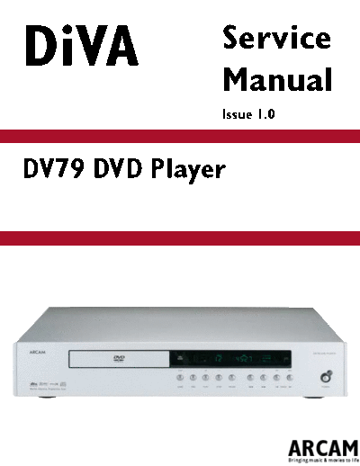
DV79 DVD Player
ARCAM
Bringing music & movies to life
DV79
Contents List
Circuit Description
Power Supply L959AY
! CCT diagram
! Component layout diagram
! Parts list
Display Board L961AY
! CCT diagram
! Component layout diagram
! Parts list
Main Board L967AY (for serial numbers below D79V03175)
! CCT diagram
! Component layout diagram
! Parts list
Main Board L974AY (for serial numbers above D79V03174)
! CCT diagram
! Component layout diagram
! Parts list
Transformers
! L924TX
! L925TX
Mechanical Assembly
! Exploded view diagram
! Mechanical and packing part list
Diva Dv79 Circuit description.
Overview
The DiVa DV/79 is a completely new design platform Fig 1 PSU clock control
and only shares it power supply board and display
board with the DV78. Fs PSUFS1 PSUFS0 PSUCLK
Frequency Pin 11 Pin 12 Output Pin 5
The player is based around acclaimed Zoran Vaddis select IC305a IC305a of IC305a
V chipset coupled to high specification Wolfson D to A 44.1 kHz 0 0 44.1 kHz
converters for all six audio output channels and a 48 kHz 0 0 48 kHz
88.2 kHz 0 1 44.1kHz
extremely high quality digital video encoder also
96 kHz 0 1 48 kHz
featured in this design is a HDMI output digital Video. 176.4 kHz 1 0 44.1 kHz
192 kHz 1 0 48 kHz
Power supply board. Others 1 1 OFF
Non-switching The PSU sync signal is driven into the power supply via
Resistor R9 if no Sync is present the unit is set to free run at
Mains power arrives at IEC inlet socket SKT1 and is xxxx due to the RT/RC network attached to Pin 4.
filtered by EMC choke LI and Y caps C3 and C4,
mains switch SW2a/b switches both Negative and Live IC1 is running in regulated mode and monitors the voltage
phases before the power reaches the mains select output on the +5V and +3V3 D.C lines, the two voltages are
switch at location SW1 the switch allows the primary summed by TR8 and Driven into the VFB and Comp inputs
windings of the transformer TX1 to be wired in either of IC1, the Voltage is then regulated by changing the time
Parallel or Series configuration. base of the PWM output at pin 6 (longer the time base the
lower the voltage), the PWM switching frequency is driven
The Bridge rectifying Diode package at location D1 into the switch-mode transformer by the high speed Nmos
forms the basis of the conventional power stage and device at position M1, R5 is used to sense the Current
supplies a VN35V6 (-35.6v) to the Switch mode across the gate of the Nmosfet and in the event of a short
stage, transistor TR1 is biased by 2v7 Zener diode circuit will safely shut the power supply down. We derive the
DZ1 and allows for the series Zener diodes DZ2, DZ3, 12v Mech supply from the output of M1 using the Ultra-fast
DZ3 to supply the VN13V5 and VN19V rails. Diode at location D8 to rectify the PWM line.
We will also see a simple A.C present circuit this is The D.C outputs from the switch mode have extensive
used for delayed output relay operation and fast relay switch mode noise removing filters these are seen as 100n
closure under interrupted supply conditions thus caps down to ground and Wire wound inductors in series
preventing power down op-amp offsets from reaching with the supply rail.
the Audio output sockets.
Power supply main board
Switch mode
All the power supply rails are supplied to the main board via
The switch mode supply is formed around the the 32 way FFC conector at location CON1001.
Driver/Control chip IC1 UC3843 (used in regulating
mode). The chip is referenced the ◦ Jabse Service Manual Search 2026 ◦ Jabse Pravopis ◦ onTap.bg ◦ Other service manual resources online : Fixya ◦ eServiceinfo