Service Manuals, User Guides, Schematic Diagrams or docs for : ARCAM DV88 Arcam-DV-88-Service-Manual
<< Back | HomeMost service manuals and schematics are PDF files, so You will need Adobre Acrobat Reader to view : Acrobat Download Some of the files are DjVu format. Readers and resources available here : DjVu Resources
For the compressed files, most common are zip and rar. Please, extract files with Your favorite compression software ( WinZip, WinRAR ... ) before viewing. If a document has multiple parts, You should download all, before extracting.
Good luck. Repair on Your own risk. Make sure You know what You are doing.
Image preview - the first page of the document
>> Download Arcam-DV-88-Service-Manual documenatation <<
Text preview - extract from the document
Service Manual DV88
Issue 2.0
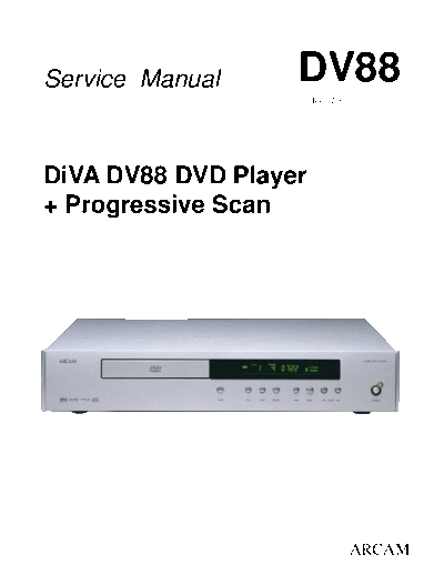
DiVA DV88 DVD Player
+ Progressive Scan
ARCAM
Contents List
! Contents list
! Circuit description
! Frequently asked questions issue 1
! Software release notes 1.1 to 1.76
! Progressive scan upgrade instructions
! Service guide
! Circuit diagrams
! Component overlays
! Circuit board parts list
! General assembly parts list
CN5 is the audio connector to the AV board. Digital audio
Circuit Descriptions in I2S and SPDIF formats are passed to the AV board from
here, as well as a number of control signals:
FSEL0..1 Selects 1 of 4 audio clock frequencies
MD, MC, ML8716_L, ML_8716_R, ML_8716_X 5 wire
SPI bus to configure audio DACs
L875 DSP Circuit GAIN_SCALING HDCD gain scaling signal.
The audio master clock also comes on to the board here. It
Summary is generated on the AV board and fed to the DSP board to
This board is used in the DV88 and DV27 DVD players. It synchronise the audio, of which more later.
can be considered to be the central digital core of the CN2 and CN3 are not fitted. They are the AV and host
player, and is based around the Zoran Vaddis III DVD interface for the AV type drive that the system was
decoder IC. A Siemens C161 microcontroller is used as originally designed to use.
the system CPU and software runs on this which controls
the whole system. A video DAC is also present, as well as Sheet 2 - CPU
an ATAPI bridge device. The system CPU, U3, is a Siemens C161 16 bit ROM-less
The board interfaces with the display board, the DVD microcontroller running at 16MHz.
drive, and the AV board. ROM and RAM are external to the micro, so we have a
CPU bus with 19 bits of address and 16 bits of data.
Overview The ROM memory is provided by U4 and U5 which
The heart of the system is the Zoran Vaddis III IC, which contain the lower and upper 8 bits of program memory
receives a data stream on its AV interface. The chip has 2 respectively. These are 28SF040 4Mbit (512K x 8)
separate DSPs, one for audio and one for video. The FLASH EEPROMs. These must be programmed and fitted
MPEG video/ audio decoding and Dolby digital audio in their sockets before the board can be tested. Once in
decoding are performed in these DSPs as well as other place they can be re-programmed in system, and the
post processing on audio and video, OSD generation, software has a feature where new software can be
decryption of DVD and other functions. uploaded from a CD. It is important to note that these
The vaddis is controlled by the system CPU via its host devices are re-programmable.
bus interface. The system RAM is provided by U6 and 7 which contain
The system uses an ATAPI type DVD drive. the lower and upper 8 bits of memory respectively. These
With the AV interface the Vaddis AV input comes directly are 1 Mbit (128K x 8) devices, making 256KByte memory
from the drive, and the drive is controlled from the system altogether.
CPU via an SSC bus (standard synchronous control). U12 is an 8 bit wide latch that provides a few extra control
The design was modified to use the ATAPI standard by output lines - these being a 5 wire serial control interface
the inclusion of the ATAPI bridge chip. This has an for the audio DACs, a reset signal for the AV drive (not
ATAPI interface to the drive, and an SSC interface to the used), and `16/9' which is used on the SCART status line.
CPU. A data stream is provided which interfaces to the U1 is a power on reset generator, this resets the micro, and
Vaddis AV input. the micro has an output RSTOUT which provides the
On the output side of the system, the digital audio output signal RESET. This goes to many devices on this board
from the Vaddis is passed to the AV board in I2S format. and the AV board and progressive scan board.
The video output from the Vaddis is in the form of a U2 is a serial EEPROM, providing non-volatile storage of
digital 8 bit parallel bus, with 27MHz clock, containing setup data. All the parameters from the setup menu are
multiplexed chroma and luma data. H and V stored here, as well as bookmarks and the region code.
synchronisation is performed by the use of embedded sync The resistor packs RP1-3, are important pullup/pulldown
patterns in the data. This type of bus is a standard interface resistors which configure the mode of the micro on power
known as BT-656. This bus connects to the video DAC, an up.
Analog Devices ADV7172. This does PAL/NTSC The resistors R2 and R12-15 are provided so we may
encoding and D-A conversion, and gives out 6 channels of configure the board for different devices. All must be
analogue video. These are composite, S-Video, and 3 lines fitted except R12 and R15 for normal configuration.
that are switchable YUV/RGB. All video outputs are
passed to the AV board where they are filtered and Sheet 3 - Vaddis DVD decoder
buffered before going to the outside world. This sheet shows the Vaddis DVD decoder IC, U8, and its
associated components.
Circuit Description Going back to the block diagram, various bus interfaces
Refer to L875 circuit diagrams were mentioned. These can be seen on the schematic as
follows:
Sheet 1 - Top level
This is the top level of the schematic and shows how the The AV interface
sheets link together plus some of the board interfaces. This is used for carrying audio/video data from the ATAPI
CN8 provides a serial port which may be connected to a bridge to the Vaddis. The following lines are used.
PC via an RS232 transceiver, for debugging purposes. DVDDAT[0:7] 8 bit parallel data
CN6 is the interface to the front panel. A 4 wire serial DVDSTRB Strobe signal
interface communicates with the VFD driver chip, which DVDSOS Start of sector indicator
drives the display, scans the buttons and drives the LEDs DVDVALID Valid data indicator
on the front panel. This interface consists of FPDIN (serial DVDREQ Request signal (Vaddis output)
data from panel), FPSEL (chip select), FPCLK (serial
clock) and FPDOUT (serial data to front panel). DVDERR is not actually used in the ATAPI configuration
IRIRQ is the signal from the IR remote receiver on the we are using.
front panel, driven by an open collector circuit. This is
because that line also goes to the progressive scan board in The HOST bus interface
the DV27, which has the remote bus input on it. The CPU uses this to control the Vaddis, it carries
CN1 is the power input. +5V and +3.3V rails are provided. information both to and from the micro.
The Vaddis and its SDRAM operate on 3.3V, everything
else runs on +5V. HD[0..7] The lower 8 bits of the system data bus
HA[1..4] Lower 4 bits of system address bus
HWR- Write strobe PSU Synchronisation
HRD- Read strobe An interesting feature of the Arcam DVD player is that the
MPGCS- Chip select switch mode supply on the PSU is synchronised to the
MPEGIRQ-Interrupt line generated by Vaddis audio sampling frequency. This is done to reduce the
switch mode noise on the audio output. The PSU will free
run on its own, when tested, but when connected to the
DSP board it will lock to the audio word clock. The signal
Digital Video bus ALRCLK is buffered by U14 to provide the signal
The 8 bit bus YUV[0:7], with CLK27 provides the BT-656 LRCK_PSU which goes to the PSU.
type parallel digital video bus. The 27MHz clock is Sheet 4 - Video DAC
provided on 2 different lines. CLK27 is used for the video This sheet shows the video encoder/DAC and output
DAC (and also goes to the ATAPI chip). CLK27PS is used buffers.
for the progressive scan board. U9 is an Analog Devices ADV7172, which does
PAL/NTSC encoding and has 6 DACs providing all our
Digital Audio video outputs.
The audio output of the Vaddis is given out on the It takes its input from the BT-656 video bus YUV[0..7],
following signals this bus is clocked by CLK27 (27MHz). No H/V sync
SPDIF-I34 IEC 958 SPDIF output signals are required since the H and V synchronisation is
ASDAT0 Serial data for Left and right done with embedded sync patterns in the data.
ASDAT1 Serial data for Lsurround, The chip has its operating parameters loaded by the system
ASDAT2 Serial data for Centre, sub CPU via the I2C bus.
ALRCLK Wordclock There are 6 analogue outputs from U9. These are
ABCLK Bit clock composite PAL/NTSC, S-Video, and 3 lines that are
configurable (via setup menu) to be YUV or RGB. The
Audio/Video clocks DACs have current outputs, so R16-21 have been chosen
Special note should be made of the audio and video clocks to give the required output level voltage, in conjunction
in the system, there are separate asynchronous clocks used with R22/24 and R23/25 which program the DAC current
for video and audio. The video runs on the system 27MHz outputs.
clock, which is generated by the Vaddis in conjunction All channels are buffered by op-amps U13,16,17. These
with the crystal Y2. have a gain of +2, and drive out to the AV board through a
The audio clock is generated on the AV board and this is source impedance of 75R. The AV board has filtering and
totally asynchronous with respect to the 27MHz clock. another buffer stage.
This is slightly unusual, since most DVD players derive There are 2 control signals that also go to the AV board
the audio clock from the video clock via a phase locked video section.
loop ENABLE_AV Used for SCART status signal. High
when player is not in standby
The Vaddis has a PLL which generates the audio clock,
but we don't use it because it has horrendous jitter. 16/9 Used for SCART status signal. High when 16:9
Instead, we bypass the Vaddis PLL and configure TV type has been selected in setup menu.
AMCLK as an input. Our clock source is on the AV board
and this is a very low jitter oscillator. Digital Video output
The Vaddis maintains AV sync by dropping or repeating 1 Connector CN4 provides a digital video output. This is
frame of video to re-synchronise the streams when they used in the DV27 only, for connection to the progressive
start to get out of sync. In practice this happens very rarely scan board.
because the 2 clocks are very accurate so the difference in YUV[0..7] are present on this connector along with clock
frequency will be very small. It is important to note that CLK27PS.
without the audio clock present, no audio or video material The system reset signal RESET- is provided, and the I2C
can be played. bus for control of devices on the progressive scan board.
The signal IRIRQ is connected to pick up the output of the
CD-DSP interface remote bus circuit which is on the progressive scan board.
(CDERR, CDFRM, CDDAT, CDCLK.) This is an open collector signal which can be driven from
The Vaddis chip has a CD-DSP interface designed to either the front panel or the remote bus input.
connect to DVD drives with this type of interface for CDs.
These signals are tracked on the board but they are not
used. The data path for CDs is exactly the same as for Sheet 5 - ATAPI Bridge and interface
DVDs. U18 is a Zoran ZR36701 ATAPI to AV port bridge.
It interfaces with the system CPU via the SSC bus, made
Reset and standby signals up of the following signals:
The signal MPGRST- is an active low signal that the
micro uses to reset the Vaddis and ATAPI bridge chip. SSC_SCLK Clock (input to ZR36701)
The signal MPGSTBY- is an active low signal that the SSC_MTSR Data input (CPU to ZR36701)
micro uses to put the Vaddis in a low power mode while SSC_MRST Data output (ZR36701 to CPU)
the player is in standby. SSC_ATN- Port ready signal (output from
ZR36701)
SDRAM DRV_IRQ- Interrupt request generated by
The Vaddis requires some memory for video and audio ZR36701
decoding and processing. This is provided by a 16MBit
synchronous DRAM (512K x 16 bit x 2 banks). The chip also receives MPGRST- to reset it from the CPU.
The board is arranged to allow 2 SDRAMs, but at present The system video clock CLK27 is connected to generate
we only use one. U11 is fitted while U10 is not fitted. The timing signals.
Vaddis interfaces directly to the SDRAM with no other
device being involved. The chip has an interface with the Vaddis referred to as the
AV interface. See the section on the Vaddis for a
description.
The ZR36701 acts as a bridge between the SSC and AV rear panel switch being set for 115V and 230V being
interfaces on one side, and the ATAPI drive on the other. applied. It is likely that the VDRs will fail short in such
The ATAPI interface of the chip connects to the DVD circumstances and will then also require replacement.
drive via 40 way IDC connector CN10.
C1 and C2 are Y capacitors which form an EMC
Signal descriptions: suppression network to common mode signals with
ATCRESET-Active low reset generated by ZR36701 to common mode choke L1. Connector SK6 provides
ATAPI drive connection for the analogue windings to the AV PCB. SK7
DD[0..15] Bidirectional data bus optionally allows a further transformer to be added to
DA[0..2] Address lines - output from ZR36701 provide the analogue supply in a more expensive model. In
CS0-,CS1- Chip selects - output from ZR36701 ◦ Jabse Service Manual Search 2026 ◦ Jabse Pravopis ◦ onTap.bg ◦ Other service manual resources online : Fixya ◦ eServiceinfo