Service Manuals, User Guides, Schematic Diagrams or docs for : Agilent HP_5065A_Manual
<< Back | HomeMost service manuals and schematics are PDF files, so You will need Adobre Acrobat Reader to view : Acrobat Download Some of the files are DjVu format. Readers and resources available here : DjVu Resources
For the compressed files, most common are zip and rar. Please, extract files with Your favorite compression software ( WinZip, WinRAR ... ) before viewing. If a document has multiple parts, You should download all, before extracting.
Good luck. Repair on Your own risk. Make sure You know what You are doing.
Image preview - the first page of the document
>> Download HP_5065A_Manual documenatation <<
Text preview - extract from the document
N&oy I--j-y-
PACkiARD
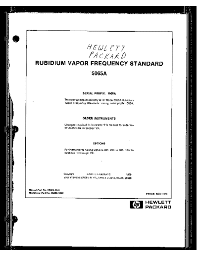
RUBIDIUM VAPOR FREQUENCY STANDARD
5065A
SERIAL PREFIX: 1909A
This manual applies directly to tlP Model 5065A Rubidium
Vapor Frequency Standards having serial prefix 1908A.
OLDER INSTRUMENTS
Changes required to backdate this manual for older in-
struments Bra in Section VII.
OPTIONS
For instruments having Options 001,002, or 003, refer to
Sections Ill through VII.
Cooyright HEWLETVACKARD 1979
530, STEVENS CREEK BLVD., SANTA CLARA, CALIF. 95050
MBmml Pad NO. 05065-9041
MiCrollChe Part No. 05065-9942 Prlnted: NOV 1979
HEWLETT
PAC:KARD
COPYRIGHT AND DISCLAIMER NOTICE
Copyright - Agilent Technologies, Inc. Reproduced with the permission of Agilent
Technologies Inc. Agilent Technologies, Inc. makes no warranty of any kind with regard
to this material including, but not limited to, the implied warranties of merchantability
and fitness for a particular purpose. Agilent Technologies, Inc. is not liable for errors
contained herein or for incidental or consequential damages in connection with the
furnishing, performance, or use of this material or data.
MANUAL CONTENTS
This manual is supplied to help you make best use of
you< instrument. The manual covers eight sections of
infocmation as follows:
Section I is an introduction to the Instrument. Elec-
trical specifications and accessories information is
given.
Section II covers inspections. power. mounting. pack-
ing, shipping, and connection.
Section III outlinesoperating procedures.
Section IV discusses technical operations.
Section V contrains disassembly and repair procedures
and an in-cabinet performance check.
Section VI lists replaceable parts.
Section VII gives options and manual changes
information.
Section VIII contains circuit diagrams, component
locators and waveforms. Included are adjustment
proceduresand troubleshooting information.
HOW TO ORDER
Y To order an operating and service manual, contact the
nearest Hewlett-Packard Sales and Service Office.
Give complete model, name. and nine-digit serial
number. The serial number plate is on the rear panel.
Comments on this manual are welcome at any Sales
and Service Office.
Model 5065A
Table of COntentS
TABLE OF CONTENTS
SOCllOn Page
I GENERAL INFORMATION ................................................... 1-i
l-l. Introduction ......................................................... l-l
l-2. Description ........................................................ l-l
1-5. Options ........................................................... l-l
i-6. Circuit Checks and Outputs ........................................ l-l
l-6. Terminology ......................................................... 1-l
l-10. Specifications ....................................................... 1-l
l-13. Instrument Identification ............................................. l-1
II INSTALLATION ............................................................. 2-1
2-I. Unpacking and Inspection ........................................... 2-i
2-3. Storage and Shipment ............................................... 2-l
2-4. Environment ....................................................... 2-1
2-6. Extended Storage .................................................. 2-l
2-6. RVFR Storage Procedure ........................................... 2-l
2-I 0. Packaging ......................................................... 2-1
2-14. Electrical Connections ............................................... 2-2
2-l 5. Power Connection ................................................. 2-2
2-l 8. Mating Connectors ................................................ 2-2
2-20. Operation as Bench or Rack Instrument .............................. 2-3
2-22. Installation Location ................................................. 2-3
III OPERATION ................................................................ 3-1
3-l. Introduction ......................................................... 3-l
3-3. Options 001 and 002 (Option 003 = 001 and 002) ...................... 3-t
3-5. Operating Procedure ................................................. 3-1
3-6. General ............................................................. 3-1
3-6. Turn-On Procedure (see Figure 3-2) ................................ 3-1
3-S. Turn-On After Long Storage ..................................... 3-1
3-10. Frequency Offset and Calibration ..................................... 3-2
3-16. Frequency Comparison Using K34-59991A Linear Phase Detector ...... 3-5
3-l 9. Operation with Time Standard Option 001 ior 003) .................... 3-9
3-22. Setting the Clock Phase to an External Clock ......................... 3-9
3-24. Automatic Synchronization ......................................... 3-9
3-26. Manual Synchronization ........................................... 3-9
3-28. Setting the Clock .................................................. 3-9
3-29. Operation with Standby Power Supply Option 002 ..................... 3-11
IV THEORY OF OPERATION ................................................... 4-1
4-I. Theory .............................................................. 4-1
4-2. General ........................................................... 4-l
4-15. Option 001, Time Standard ........................................... 4-2
4-20. Option 002. Standby Power Supply ................................... 4-3
V MAINTENANCE ............................................................. 5-I
5-l. Introduction ......................................................... 5-1
5-5. Instrument Access ................................................... 5-l
5-7. Periodic Maintenance ................................................ 5-l
5-6. Instrument Troubleshooting .......................................... 5-6
5-9. Introduction ....................................................... 5-6
5-15. Fault Finding ...................................................... 5-7
5-19. Loop Alignment Procedure ........................................... 5-12
5-20. Introduction ....................................................... 5-l 2
5-22. t20 Volt Adjustment (A15 Power Supply and
Regulator Assembly) ............................................... 5-12
5-24. A10 Frequency Adjustment ......................................... 5-12
5-25. RFAlignmant ...................................................... 5-13
5-26. Signal-to-Noise Ratio .............................................. 5-14
5-27. Modulation Frequency Adjustment .................................. 5-14
5-28. Phase Adjustment Recheck ......................................... 5-14
iv
Model 5065A
Table of Contents. List of Figures
TABLE OF CONTENTS (Continued)
SectIon Page
VI
VII
VIII
LIST OF FfGURES
FlgUre IPage
1-i.
2-1.
2-2.
3-l. RVFR Pumping .............................................................. 3-2
3-2. Turn-On Procedure .......................................................... 3-3
3-3. Magnetic Field Control ....................................................... 3-5
3-4. Error Measurement .......................................................... 3-5
3-5. Equipment Setup for Calibrating Phase Measurement System .......... ....... 3-7
3-6. Equipment Setup to< Frequency Difference Measurement ...................... 3-0
3-7. Internal Measurement with AutQmatic Synchronization ... .*, .................. 3-12
3-8. Internal Measurement with Manual Synchronization ................... ... t ... 3-12
3-9. Front Panel Controls ......................................................... 3-13
3-10. Rear Panel Operating Controls .................... *. ................. ....... 3-14
3-l 1. TopOperating Ccntfols ...................................................... 3-15
4-l. Rubidium Absorption Plot ............................................ . ....... 4-1
4-2. Rbat Absorption Cell Output ........................................... ..ll .. 4-2
4.3. RVFR Assembly Block Diagram .............................................. 4-3
5-1, A8TP3 Waveform at 200 X 10-X and Phase Misadjusted ............... ....... 5-2
5-2. A8TP3 Waveform at 200 X 10 -10 and Phase Correct , ......................... 5-2
5-3. Harmonic and Non-Harmonic Distortion Test Setup .................. _, ....... 5-3
5-4. Equipment Setup for Synchronization and Delay Checks ...................... 5-4
5-5, 5 MHz Output Stability Test Setup ............................................ 5-5
5-6. 5065A Simplified Block Diagram .................. ,. .......................... 5-7
5-7. Meter Response in ERROR Position .............. .................. _, ....... 5-10
5-6. Waveform at A8TP3 with Severe Phase Shift .................................. 5-12
5-9. R.F.AlignmentSetup ........................................................ 5-13
5-10. Oscilloscope Indication at Resonance with A8R43 (Modulating Phase
Adjustment) Correctly Adjusted ............................................ 5-13
5-11. Signal-to-Noise Test Setup ... ............................................... 5-14
6-l.
Model 5065A
List of Figures
FIgwe
7-i.
7-2. A2 Bakery Charger Assembly ................................................. 7-3
73. 100 kHz Regenerative Divider ................................................ 7-8
7-4. A4 100 kHz Divider .......................................................... 7-i 1
7-5. A4 100 kHz Frequency Divider Assembly ...................................... 7-11
7-E. Al Waveforms ............................................................... 7-21
7-7. Synthesizer Assembly Al Block Diagram ...................................... 7-21
7-B. Al Synthesizer Assembly .................................................... 7-23
7-9. Part of Al Synthesizer Assembly ............................................. 7-23
7-10. Al Waveforms ............................................................... 7-25
7-11. Synthesizer Al Phase-Locked Oscillator Section .............................. 7-25
7-12. A7 AC Amplifier Component Locator ......................................... 7-35
7-l 3. A7 AC Amplifier Schematic Diagram .......................................... f-35
r-14. Top Operating Controls ...................................................... 7-37
7-15. A5 Digital Divider Assembly (Option 001) ..................................... 7-39
7-16. A16 Digital Divider Power Supply Assembly ................................... 7-41
7-17. Al9 LED Digital Clock Assembly ............................................. .7-51
7-16. TopOperating Controls ...................................................... 7-53
7-19. A5 Digital Divider Assembly .................................................. 7-55
7-20. Al6 Digital Divider Power Supply Assembly ................................... 7-57
8-l. Schematic Diagram Notes .................................................... 8-2
8-2. Block Diagram .............................................................. 8-3
0-3. Front and Rear Panel and Top Internal Views ................................. 8-4
a-4. Wiring Diagram (Sheet 1 of 3) ................................................. 8-5
0-5. Bottom Internal View ........................................................ 6-6
8-8. Wiring Diagram (Sheet 2 of 3) ................................................ 8-7
6-7. Wiring Diagram (Sheet 3 of 3) ................................................ 8-9
8-9. Synthesizer Assembly Al Block Diagram Digital Section ....................... 8-11
6-9. Synthesizer Assembly Al Digital Section (Sheet 1 of 2) ........................ 8-17
8-Q. Synthesizer Assembly Al Phase-Locked Oscillator Section (Sheet 2 of 2) ....... 8-19
8-10. A2 Battery Charge Assembly (Option 002 and 003) ............................ 8-21
8-11. A3 Multiplier Assembly ....................................................... 8-25
6-12. A4 100 kHz Frequency Divider ................................................ 8-27
8-13. A5 Digital Divider Assembly (Optiotl 001) (Sheet 1 of 3) ....................... 8-33
8-l 4. A5A2 Master Clock Board [Option 001) (Sheet 2 of 3) ......................... 6-35
8-15. A5A3 Preset Clock Board (Option 001) (Sheet 3 of 3) .......................... 8-37
8-16. A6 1 MHz Frequency Divider Assembly ....................................... 8-41
8-17. A7 AC Amplifier Assembly ................................................... 8-43
8-16. A0 Phase Detector Assembly ................................................. 847
B-19, A9 Integrator Assembly ...................................................... 8-49
8-20. A10 Oscillator Assembly Block Diagram ...................................... 8-53
8-21. All RVFA Temperature Controller Assembly .................................. 8-55
8-22. Al2 RVFR Assembly and Buffer A13 Amplifier Assembly ....................... 8-59
0-23. Al4 Logic Assembly ......................................................... 8-63
a-24. A15 Power Supply and Regulator Assembly ................................... 8-65
6-25. Al6 Digital Divider Power Supply Assembly ................................... 8-67
8-26. A19 Series 1740 Digital Clock Schematic Diagram ............................. 8-71
vi
1-2. Accessones AvaIlable ........................................................ l-2
1-3. Specifications ............................................................... l-3
2-l. 1151230 Volt Conversion ..................................................... 2-2
2-2. Mating Connectors .......................................................... 2-3
3-1. Operating Checks ........................................................... 3-1
3-2. Front Panel Lamp Indications ................................................ 3-4
3-3. Frequency Offset Change Instructions ........................................ 3-E
3-4. Typical Frequency Offset Change. Sample ~lnsufficient
MAGNETIC FIELD Control') ................................................ 3-7
3-5. Typical Frequency Offset Change. 0X10-10 Offset to -300X10-10 ............... 3-6
3-6. Offset Frequency Settings .................................................... 3-10
3-7. Synthesizer Setting vs. Frequency Offset ...................................... 3-l 1
3-6. Recommended Test Equipment ............................................... 3-11
4-1, Logic Signals ................................................................ 4-3
5-l. Asssmbly Designations ...................................................... 5-l
5-2. In-Cabinet Performance Check ............................................... 5-2
5-3. Circuit Checks .............................................................. 5-6
5-4. Signal Checks ............................................................... 5-10
5-5. Recommended Test Equipment ............................................... 5-l 1
5-6. A5 Troubleshooting .......................................... .`*, ............. 5-17
6-1, Table of Abbreviations ....................................................... 6-1
6-2. Replaceable Parts ........................................................... 6-3
6-3. Option 002 and 003 Replaceable Parts ........................................ 6-21
6-4. Option 001 Replaceable Parts ................................................ 6-23
6-5. Options 001. 003 Only Replaceable Parts ..................................... 6-27
6-6. ManufacturersCode List ..................................................... 6-31
7-I. Manual Changes ............................................................. 7-1
7-2. Battery Charger Replaceable Parts ........................................... 7-5
7-3. A4 100 kHz Divider Replaceable Parts ........................................ 7-13
7-4. Al Synthesizer Assembly Replaceable Parts ................................... 7-17
7-5. Al Troubleshooting .......................................................... 7-26
7-6. Al Troubleshooting .......................................................... 7-27
7-7. Al Troubleshooting
7-7. Al Troubleshooting .......................................................... 7-28
7-a. A1 Troubleshooting .......................................................... 7-29
7-Q. A7 AC Amplifier Assembly Replaceable Parts ................................. 7-32
7-10. A16 Resistor Parts List ....................................................... 7-38
7-11. Al6 Resistor Parts List ....................................................... 7-52
7-12. A5A4 Parts List .............................................................. 7-58
Model 6065A
Circuit Diagrams, Theory, and Maintenance
Flmwe 1-l. Mndnl5065A and Accessories
Shown with Option 003 (001 + 002 = 003)
AC POWER CORD RACK MOUNT KIT
ACCESSORY KIT
Model 506549
Circuit Diagrams, Theory, and IMaintenance
SECTION I
GENERAL INFORMATION
1-l. INTRODUCTION l-8. TERMINOLOGY
I-2. Description l-9. The definitions of the following terms apply to
these terms as used throughout this manual.
l-3. The Hewlett-Packard Model 5065A Rubidium
Vapor Frequency Standard is a compact, self-contained a. ATOMIC TIME. Time scale ba:jed on the
secondary frequency standard which uses an optically- hyperfine resonance of Cesium 133.
pumped Rubidium vapor cell as the reference element.
A 5 MHz oscillator is stabilized against a natural b. UNIVERSAL TIME (UT2). Time scale based
atomic r*SO"a"C*. the hyperfine transition of on the earth's rotation about its axis with correction
Rubidium 07. This technique produces a long-term for angular position and seasonal variations: proceeds
stability of better than 1 x 10 -I' per month with at a rate slightly slowerthan Atomic time.
excellent short-term stability which is conservatively
rated at less than 5 x IO-`* rms averaged over a one- c. UNIVERSAL TIME (COORDINATED) (UTC). A
second period. Output frequencies are 5 MHz. 1 MHz, piecewise uniform scale which approximates UT2 to
and 100 kHz. 0.1~second by step adjustments in phase as announced
by the Bureau International de I'Heure in Paris.
l-4. Frequency setting for any Offset Of the UTC time
reference is accomplished by changing the microwave
excitation frequency and the magnetic field applied d. HYPERFINE RESONANCE OF Rbs'. Hyper-
10 an Rb"' vapor cell. Thumbwheel switch control fine resonant frequency arising from the difference
(of a digital frequency synthesizer) provides approxi- in energy between the upper and lower ground states
mate step adjustment of the microwave excitation fre- of Rbs'.
quency with a range of 1000 parts in 10'O. In addition,
the front-panel MAGNETIC FIELD control provides e. RVFR (Rubidium Vapor Frequency Reference).
for exact adjustment of the RbB' hyperfine transition The assembly which houses the RbO' lamp, filter cell.
with a resolution of 2 parts in 10'2. the Rbsr absorption cell, and the harmonic generator/
mixer diode.
l-5. options
a. A digital clock, Option 001. provides a clock dis-
l-10. SPECIFICATIONS
play and a one pulse per second (1 PPS) electrical output.
The clock pulse may be retarded up to l-second in incre-
l-11. Table 1-3 lists the technical specifications for
ments as small es l-microsecond and as large as 0.1. the Model 5065A.
second. In addition, a separate control provides Contin-
uous adjustment of clock-pulse delay from O- to I- l-12. Table l-l lists equipment supplied and Table
microsecond. I-2 lists accessories available for the Model 5065A.
b. Standby battery, Option 002, provides a IO-
minute minimum power source (at 25◦ Jabse Service Manual Search 2024 ◦ Jabse Pravopis ◦ onTap.bg ◦ Other service manual resources online : Fixya ◦ eServiceinfo