Service Manuals, User Guides, Schematic Diagrams or docs for : Casio Cameras CASIO_QV_10B
<< Back | HomeMost service manuals and schematics are PDF files, so You will need Adobre Acrobat Reader to view : Acrobat Download Some of the files are DjVu format. Readers and resources available here : DjVu Resources
For the compressed files, most common are zip and rar. Please, extract files with Your favorite compression software ( WinZip, WinRAR ... ) before viewing. If a document has multiple parts, You should download all, before extracting.
Good luck. Repair on Your own risk. Make sure You know what You are doing.
Image preview - the first page of the document
>> Download CASIO_QV_10B documenatation <<
Text preview - extract from the document
(with price)
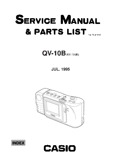
QV-10B(KX-720B)
JUL. 1995
R
CONTENTS
SPECIFICATIONS ......................................................................................... 1
BLOCK DIAGRAM ........................................................................................ 2
CIRCUIT OPERATION .................................................................................. 3
ADJUSTMENT ............................................................................................. 13
DISASSEMBLY AND ASSEMBLY .............................................................. 17
PRINTED CIRCUIT BOARDS ..................................................................... 18
ELECTRICAL PARTS LIST......................................................................... 20
MECHANICAL PARTS LIST ....................................................................... 30
EXPLODED VIEW ....................................................................................... 31
PARTS LIST FOR ACCESSORIES ............................................................. 32
REPAIR METHOD ....................................................................................... 33
SCHEMATIC DIAGRAMS ........................................................................... 35
WAVEFORMS.............................................................................................. 38
SPECIFICATIONS
Item Specification
1. Recording System Digital (JPEG based)/Field recording
2. Signal System NTSC
3. Recording Medium Built-in 16-Mbit flash memory
4. Number of pages 96
5. Delete Functions Single page; All pages (with page protect feature)
6. Imaging Device 1/5-inch CCD (Total Number of Pixels: 250,000)
7. Lens Fixed focus with macro position; F2/f = 5.2mm
8. Aperture F2/F8 manual switching
9. Focal Length F2/NORMAL : 60cm to 310cm;
F2/MACRO :13cm to 16cm
F8/NORMAL :28cm to ;
F8/MACRO :10cm to 24cm
(from lens protection filter)
10. Light Metering TTL center point by photographic element
11. Exposure Metering Aperture priority AE
12. Exposure Range EV +5 to 18
13. Exposure Adjustment -2EV to +2EV
14. Shutter System Electronic
15. Shutter Speed 1/8 to 1/4000 second
16. White Balance Automatic
17. Self-timer 10-second
18. Monitor 61,380-pixel 1.8-inch TFT low-glare color LCD;
doubles as finder
19. Terminals DIGITAL; VIDEO OUT; DC IN 6V
20. Power Supply Batteries (AA-size Alkaline batteries X 4)/AC Adap-
tor (AD-C60)
21. Battery Life Approximately 120 minutes
22. Dimensions 66(H) X 130(W) X 40(D)mm /
2.6" (H) X 9" (W) X 1.6" (D)
23. Weight Approximately 190g / 6.7oz (excluding batteries)
24. Accessories Wirst strap; soft case; special video cable; AC adap-
tor (AD-C60) Alkaline batteries (LR6 X 4); cleaning
cloth; owner's manual; personal computer connec-
tion kit
--1--
BLOCK DIAGRAM
1 Camera PCB 2 Digital PCB 3 Linear PCB
V RAM IC300
Gate Array HM53812BJ8 IR3P90Y
CCD
HG51B167FB LCD
IC400
MSM6770GS
Flash
Memory
TC5816FT-1 5 VIDEO OUT (Video I/O)
D RAM
HM514B00
ALJ8
CPU
HD6477034F16 6 DIGITAL (Serial I/O)
Power Supply
Circuit
DC IN (6V)
Key
AC adaptor
Battery x 4 Key PCB
1 Camera Unit: It is used to provide color information.
2 Digital PCB: It controls the CCD, compressed data, stores image in memory.
3 Linear PCB: It generates the tricolor and controls the LCD display.
4 LCD: 61,380-pixel 1.8-inch Thin Film Transistor low-glare color LCD.
5 VIDEO OUT(Video I/O): Use this terminal when connecting to the VIDEO IN terminal of
a TV, video tape deck, video printer, or other similar device.
6 DIGITAL (SERIAL I/O): Use this terminal when connecting to a personal computer.
--2--
CIRCUIT OPERATIONS
CAMERA UNIT (CAMERA PCB)
The camera unit is composed a lens, color filter, CCD (IC802), driver (IC800) and signal
processor (IC802). It produces voltages R, B, and G, for the colors red, blue, and green
when light from a scene is focused on the surface. These voltage values vary according
to the intensity of the respective color being scanned.
The camera unit must be replaced with whole unit when it is defective, because the precise
adjustment is required when the individual parts are replaced, and can be done only at our
factory.
Camera PCB Digital PCB
Data Bus
1 Lens 4 IC801
3 IC802 (CCD)
Ye,Cy,Gr
color signal Sample Hold, 8bit A/D D0 ~ D7
AGC Converter
CCD IN D RAM
2 Color PHI1~PHI4
Filter PHS1~PHS4
IC800
Driver
Timing CPU
VI1~ VI4 Generator MCK,
VS1 ~ VS4 HRS2,
FTTRG,
STTRG,
CCODE,
ENDFLG
1 Lens
Concentrates light rays to a point.
2 Color filter
The striped color filter in front of the CCD detector is used to provide color information.
It has three colors, yellow, green and cyan.
Array of color filter and signal processing (IC801) for camera are extremely close relationship.
1 2 3 ~ 506 507 508
Ye G Cy Ye G Cy
Red
Ye G Cy Ye G Cy Ye=Red+Green Mg=Blue+Red
Ye Mg
Ye G Cy Ye G Cy
White
Ye G Cy Ye G Cy Cy
Green Blue
Ye G Cy Ye G Cy
Cy=Blue+Green
Array of color filter Three Primary colors
--3--
3 CCD (IC802)
A charge-coupled device in which charges are introduced when light from a scene is
focused on the surface of the device. The image points are accessed sequentially to
produce a television-type output signal.
Effective picture element:
532(H) 249,936 = 508 (H) x 492 (V)
508(H)
PHI4 PHIS1~PHIS4:
3 Clock pulse for the storage.
PHI3
4
5 PHI2
492(V)
500(V)
PHI1 Image pickup PHI1~PHI4:
6
Clock pulse for the image pickup.
PHIH1~PHIH2:
Clock pulse for the horizontal shift
PHIS4 19 register.
PHIS1 18
PHIR 7
Storage PHIS2 17 PHIR:
PHIS3 16 CCD analog signal output.
VDD 8
Amp.
Output
Horizontal shift
Vout 9
register (CCD)
PHIH1
PHIH2
VOG
VGG
12 13 14 15
4 Camera Signal Processor (IC801)
D0~D7:
D0~D7 Digital signal of the luminance and the
Sample Hold, 8bit A/D
AGC Converter color difference B-Y and R-Y signal.
From CCD
CCD IN:
CCD analog signal input.
VI1~VI4/VS1~VS4:
Clock pulse for the CCD control signal.
Timing
Generator
to CCD From/to CPU
Sample Hold
Selects a desired signal from the CCD.
Timing Genarator
Generates the clock pulse for the CCD.
8-bit AD converter
Analog signal from the CCD is converted into 8-bit digital signal of the luminance and the color
difference B-Y and R-Y signal. .
--4--
DIGITAL PCB
Camera PCB
IC802
CCD
IC801 2 IC700 Gate Array
3 IC701
Control V RAM
IC800 Processor
Timing Control
1M
Driver
V RAM
Encoder
4 IC602 Data
Compre- Amp.
16M Flash Memory ssor
D/A
VIDEO OUTPUT
(Video I/O)
DIGITAL PCB 1 IC600 Microprocessor
ROM RAM
Linear
PCB
DMAC
5 IC601 IC300
Chroma TFT LCD
4M D RAM CPU Circuit
+5V +18V -10V
BSC
IC400
6 Display
Power Supply SCI, Timmer Control
I/O Port DIGITAL (Serial I/O)
DC in +6V
Key Input
Battery
Digital PCB is composed Microprocessor (IC600), D RAM (IC601), Flash Memory (IC602),
Gate Array (IC700), and V RAM (IC701).
Microprocessor controls the CCD, D RAM, Flash Memory and key operation. Gate array
compresses data for the color and the luminance from the CCD to increase the number of
memory, and up to 96 images can be stored in flash memory. The color and the luminance
data are mixed in the gate array to make the video signal.
As to spare parts for digital PCB, Casio supplies PCB ass'y and the individual parts.
--5--
1 CPU (IC600)
Controls the CCD, D RAM, Flash memory and key operation.
PA15 ~ PA0 CS3 ~ CS0, A21 ~ A16
Port A Address
PROM/MASKROM1 RAM1
Reset,
MD2 ~
MD0,
EXTAL,
Address
XTAL
A15 ~ A0
CK
Direct memory
CPU access
controller
Interrupt User break
controller controller Direct state controller
Serial communication 16-bit integrated
interface (x2channel) timer pulse unit
Data/Address
Programmable timing A/D Timer
pattern controller converter AD15 ~ AD0
Port C Port B
PC7 ~ PC0 PB0 ~ PB15
Address bus 24-bit Address bus 24-bit
High-order 8-bit
Data bus 16-bit
Low-order 8-bit
--6--
CPU PIN FUNCTION
Pin No. Terminal Name IN/OUT Function
1 PB14 OUT Timing pattern output.
2 PB15 - Not used.
3 VSS IN Ground terminal.
4 - 11 AD0 - AD7 IN/OUT Address bus.
12 VSS IN Ground terminal.
13 - 14 AD8 - AD9 - Not used.
15 VCC IN Power source.
16 - 21 AD10 - AD15 - Not used.
22 VSS IN Ground terminal.
23 - 30 A0 - A7 OUT Address bus.
31 VSS IN Ground terminal.
32 - 33 A8, A9 OUT Address bus.
34 - 39 A10 - A15 - Not used.
40 VSS IN Ground terminal.
41, 42 A16, A17 - Not used.
43 VCC IN Power source.
44 - 47 A18 - A21 - Not used.
48 - 50 CS0 - CS2 - Not used.
51 CASL OUT CAS(Column Address Strobe) signal for D RAM.
52 VSS IN Ground terminal.
53 PAO - Not used.
54 RAS OUT RAS(Row Address Strobe) signal for D RAM.
55 CS6 OUT Chip select signal.
56 WAIT - Not used.
57 WR OUT Write enable signal for outer memory (low-order 8-bit).
58 PA5 OUT Write enable signal for outer memory (high-order 8-bit).
59 RD OUT Read enable signal for outer memory.
60 PA7 - Not used.
61 VSS IN Ground terminal.
62 PA8 IN Bus request signal.
63 PA9 OUT Interrupt request signal.
64 - 66 PA10 - PA12 - Not used.
67 DREQ0 IN Interrupt request signal.
68 IRQ2 IN Interrupt request signal.
69 PA15 IN Interrupt request signal.
70 VCC IN Power source.
71 CK OUT System clock pulse.
72 VSS IN Ground terminal.
73 EXTAL IN Clock pulse input.
74 XTAL - Not used.
75 - 77 VCC, NMI, VPP IN Power source.
78 WDTOVF - Not used.
79 RES IN Reset signal input.
80 MD0 IN Ground terminal.
81 MD1 IN Connected to VCC3.
82 MD2 IN Connected to ground.
83, 84 VCC IN Power source.
--7--
Pin No. Terminal Name IN/OUT Function
85, 86 AVCC, AVREF IN Connected to VCC3.
87 - 89 PC0 - PC2 IN Key input terminal.
90 PC3 IN Low battery detection terminal.
91 AVSS IN Ground terminal.
92 - 95 PC4 - PC7 - Not used.
96 VSS IN Power source.
97, 98 PB0, PB1 IN/OUT Port B.
99 VCC IN Power source.
100 - 105 PB2 - PB7 IN/OUT Port B.
106 VSS IN Ground terminal.
107 RXDO IN Data input terminal from a personal computer.
108 TXDO OUT Data output terminal to a personal computer.
109, 110 PB10, PB11 IN/OUT Port B.
111 PB12 - Not used.
112 PB13 - Not used.
2 Gate Array (IC700)
Control V RAM
Timing Control
V RAM
Encoder
Data
Compressor
D/A
Data Compressor
The color difference and the luminance data is compressed about 1/7 to increase the
numer of images in memory. Up to 96 images can be stored.
Y (luminance siganal) data : 480 x 224 byte
Cb (color difference signal B-Y) data : 160 x 112 byte 21,120 byte
Cr (color difference signal R-Y) data : 160 x 112 byte 1/7
Total: 143,360 byte 21,120 byte
Encoder
The color and the luminance data are mixed internally to make the video signal, and
send it to the linear PCB and the video out terminal.
--8--
3 V RAM
It is used for encoder function.
4 Flash Memory
Up to 96 images can be stored in memory. Flash memory does not require electrical power
to store data, so image data is retained in memory even when you turn camera power off.
If batteries go dead, simply load a set of new batteries or connect the AC adaptor and you
will be able to view images in camera memory.
Memory Map
Header Image data Color
record Max; 96 images Information
5 D RAM
There is area of work space that the microprocessor uses for storing temporary data , the
intermediate results of calculations, and all sorts of pieces of information that the system
needs to remember.
6 Power Supply
Terminal Voltage Purpose
VCC3-0 4.75 ~ 5.15 (V) Logic circuit
VCC3-1 4.70 ~ 5.15 (V) Video output
VCC3-2 4.60 ~ 5.15 (V) Digital I/O
VCC6 17.80 ~ 18.20 (V) CCD
VEE3 -9.6 ~ -10.6 (V) CCD
KEY PCB
Block Diagram
BUTTON RESISTOR CPU
KEY 0
87 pin
KEY 1
VCC3-1 88 pin
KEY 2
89 pin
Key Matrix
VOLTAGE BUTTON RESISTOR KEY MATRIX CPU
VCC3-1 Shutter R900(1.8K) KEY0 87pin
VCC3-1 [+] R901(15K) KEY0 87pin
VCC3-1 MODE R902(1.8K) KEY1 88pin
VCC3-1 DISP R903(4.7K) KEY1 88pin
VCC3-1 ZOOM R904(10K) KEY1 88pin
VCC3-1 SELF R905(27K) KEY1 88pin
VCC3-1 [-] R906(1.8K) KEY2 89pin
VCC3-1 DEL R907(15K) KEY2 89pin
--9--
LINEAR PCB
IC300 generates the tricolor (red, green and blue) from the video signal, and IC400 controls
the TFT-LCD display.
Power Supply
Terminal Voltage Purpose
VCC2 4.3 ~ 4.7 (V) Logic circuit
VCC4 9.5 ~ 11.0 (V) Display
VEE2 -7.0 ~ -8.0 (V) Display
VEE4 -16.5 ~ -17.9 (V) Display
TIME-CONST
IC300
SYNC-OUT
SYNC-SEP
AGC OUT
PICTURE
SYNC-IN
H.F.OUT
AGC.FIL
COLOR
CLAMP
DCDET
G-OUT
R-OUT
B-OUT
TRAP
APL
18 15 19 20 21 22 16 11 17 14 13 23 35 32 34 36
42
Vref
SYNC SEP
BGP GEN AGC DET
H filter RGB.
VIDEO 38 AMP
10 Trap D.L CLAMP AGC AMP
F ADJ INV INV INV 41
12
44
ACC BPF Color control 2
corrector
45
ACC.F
Picture corrector 1
9 ACC DET quality
ADJ. corrector
APC.F 46
27 APC Killer
SWP GEN
24
Killer.F RGB.
26 L INV
VCO Matrix INT/EXT R Gain 40
VCO Demodulation P Clamp
Contrast SW 39
F Bright
B Gain FRP
28
TINT COM.
VEE VCC1 GND VCC2 VEE
COM DRIV AMP
25 7 6 29 33 31 2 5 4 3 1 48 47 43 30
GND
R-SUB-CONT
VCC2
EXT-G
EXT-B
B-SUB-CONT
BRIGHT
COM.OUT
CONT
SW
VCC1
EXT-R
VEE
TINT
YEE
-- 10 --
M1~M7
GPCK
GRES
IC400
GSRT
MBUI
HDB
UHF
KCB
KDB
CLR
AVB
SRT
AFT
OE
U/V
Key control
51
VCO 39 AFTO
VCO 46 VREF
ADJ AFT
48 45 U1
control Analog 44 VH1
5.9MHz
control 43 VL1
47 Clock CKB
OSC Mode control 41 OUT
SW Horizontal
control
SYF 18 PHO Mode Tuning program
Control 35
50 set control VMUTEB
PD PD
POCL VTUCK
LOE0
CK2
Channel 34 SW
Tuning Up/Down 32
VBAR
CK2 Initial counter bar control 33
1/2 UBAR
PL1, PL2, PL3
30
PDM D/A TUPCM
56 29
MCLK Amplitude TAB/COG VLB
control SW
SELFRB SD
VD
TSI1 54
SYNC
TSI2 55
Vertical judgment SYNC SYNC
TSI3 8
Test Test
control
TSI4 9 circuit VSync SEP. DET.
TSI5 10 HSync
TSI6 11 Mute
24 36 2 28 38
VDB FRP HCNT AMUTEB CSYNC
-- 11 --
TFT-LCD
Selective period Source electrode Gate electrode
Gate Frame period
pulse
Vy t1
Y1 Y1
T1 T2 T3 T4 Tn
GND Picture
element A
Y2
Y2
Y3 Y3
Va
X1 Vb
Ym
t1 t2 t3
X1 X2 X3 X4 Xn
TFT array substrate Common substrate
Picture Common
element electrode
A V COM
Each picture element electrode is controlled by a transistor. To the gate electrodes, the
gate pulse is applied timesharing. VCOM voltage is applied to the common electrodes.
The above figure shows the operation of TFT-LCD. If the gate pulse is not applied to
the gate electrodes, the transistors do not operate even when the potential difference
is given between the common electrodes and source electrodes, and no effect is given
to the liquid crystal. If the gate pulse is applied to Y1, the transistorT1 is in operation
during a priod of t1, and voltage of source electrode of Va is applied to the LCD layer
of picture element A, then electric charges are stored in the picture element of A. After
the period of t1, T1 is turned off, and voltage in the LCD layer of A is held until next
gate pulse comes, but it drops little by little through off leak resistance of TFT and leak
resistance of LCD itself.
BACK LIGHT
The camera unit is equipped with a fluorescent light source to provide the back lighting
for its LCD. The normal service life of the backlight is approximately six years, when the
camera is used for about two hours a day.
The backlight is consumption items, so even under guarantee replace it under charge
basis.
-- 12 --
ADJUSTMENT
LINEAR PCB
Items to Be Adjusted
Item Measuring Instrument
VCC2 voltage setting Voltmeter, Regulated power supply
VBL voltage setting Voltmeter, Regulated power supply
Vcom adjustment Patern generator, Oscilloscope, Regulated power supply,
Photo sensor amp., Band pass filter
Free-running Frequency Pattern generator, Oscilloscope, Regulated power supply
adjustment
Bright and Contrast adjustment Pattern generator, Oscilloscope, Regulated power supply
Color adjustment IBM PC, Cable for LK-1, Light source, Color filter,
Color adjustment program
Adjustment and Test Point Locations
CP302
VR303
CP410
VR300
VR302 CP108
CP412 VR100
VR101
CP111
VR400
VR304
Top View
-- 13 --
Equipment Connection / Adjustment Procedure
VCC2 Voltage Setting
Regulated
power QV-10
supply Set Voltmeter
Input Output
DC Jack CP108
5.0 ◦ Jabse Service Manual Search 2026 ◦ Jabse Pravopis ◦ onTap.bg ◦ Other service manual resources online : Fixya ◦ eServiceinfo