Service Manuals, User Guides, Schematic Diagrams or docs for : DENON Network Audio Video Player Network Audio Video Player Denon - DN-V200 & V300 Схема DN-V200 & V300
<< Back | HomeMost service manuals and schematics are PDF files, so You will need Adobre Acrobat Reader to view : Acrobat Download Some of the files are DjVu format. Readers and resources available here : DjVu Resources
For the compressed files, most common are zip and rar. Please, extract files with Your favorite compression software ( WinZip, WinRAR ... ) before viewing. If a document has multiple parts, You should download all, before extracting.
Good luck. Repair on Your own risk. Make sure You know what You are doing.
Image preview - the first page of the document
>> Download Схема DN-V200 & V300 documenatation <<
Text preview - extract from the document
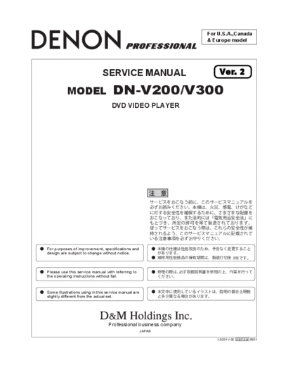
                                                                  For U.S.A.,Canada
                                                                  & Europe model


                              SERVICE MANUAL                              Ver. 2

           MODEL                    DN-V200/V300
                                   DVD VIDEO PLAYER


For purposes of improvement, specifications and
design are subject to change without notice.


Please use this service manual with referring to                     ,
the operating instructions without fail.


Some illustrations using in this service manual are
slightly different from the actual set.


                                  Professional business company
                                                      JAPAN

                                                                         X-0201 V.02 DE/CDM 0501
                                              DN-V200 / V300


SAFETY PRECAUTIONS

LEAKAGE CURRENT CHECK


LASER RADIATION


                                  500V


                                         1M


(1)


(2)


                            (1)

                            (2)


                        2
                    DN-V200 / V300

BLOCK DIAGRAM


                3
                                                                                         DN-V200 / V300

SEMICONDUCTORS
 Only major semiconductors are shown, general semiconductors etc. are omitted to list.

   IC's

 ST72321   (IC 01)


                                                       4
                                                                                        DN-V200 / V300
BU2098F    (IC 02)


NJM2068 (IC 03)                                                       74VHC04 (IC 05)


ST202EBW (IC 09)
  PIN CONFIGURATION


  PIN DESCRIPTION

          PlN No      SYMBOL                      NAME AND FUNCTION
            1          C1+     Positive Terminal for the first Charge Pump Capacitor
            2           V+     Doubled Voltage Terminal
            3           C1-    Negative Terminal for the first Charge Pump Capacitor
            4          C2 +    Positive Terminal for the second Charge Pump Capacitor
            5           C2-    Negative Terminal for the second Charge Pump Capacitor
            6            V-    Inverted Voltage Terminal
            7          T2OUT   Second Transmitter Output Voltage
            8          R2IN    Second Receiver Input Voltage
            9         R2OUT    Second Receiver Output Voltage
           10          T2IN    Second Transmitter Input Voltage
           11          T1IN    First Transmitter Input Voltage
           12         R1OUT    First Receiver Output Voltage
           13          R1IN    First Receiver Input Voltage
           14          T1OUT   First Transmitter Output Voltage
           15          GND     Ground
           16          VCC     Supply Voltage


                                                    5
                                     DN-V200 / V300

KA78L08A (IC 21)


    1.Output


                       3.Input
               2.GND


KA79L08A (IC 22)
    1.Output


                       3.Input
               2.GND


                                 6
                       DN-V200 / V300

BH7862FS (IC 61)


BA7660FS (IC 62)


                   7
                        DN-V200 / V300

PT6315V18 (IC 71)


  BLOCK DIAGRAM


                    8
                                      DN-V200 / V300

  FL DISPLAY HNV-06SC15T (FIP1)


PIN CONNECTION


GRID ASSIGNMENT


ANODE CONNECTION


                                  9
 PRINTED WIRING BOARDS                                  DN-V200 / V300

CUP11793   FRONT A/V UNIT ASS'Y   COMPONENT SIDE


                                                   10
                                                 DN-V200 / V300

CUP11793 FRONT A/V UNIT ASS'Y   FOIL SIDE


                                            11
                                                DN-V200 / V300


RL-S874 MECHANISM UNIT ASS'Y
COMPONENT SIDE                      FOIL SIDE


                               12
                                         DN-V200 / V300

 CUP11794Z SMPS UNIT ASS'Y
COMPONENT SIDE               FOIL SIDE


                             13
                                                                                                                                                                                             DN-V200 / V300


NOTE FOR PARTS LIST
  l Part indicated with the mark " " are not always in stock and possibly to
     take a long period of time for supplying, or in some case supplying of
     part may be refused.
  l When ordering of part, clearly indicate "1" and "I" (i) to avoid mis-
     supplying.
  l Ordering part without stating its part number can not be supplied.
  l Part indicated with the mark " " is not illustrated in the exploded view.
  l Not including Carbon Film Resister
◦ Jabse Service Manual Search 2026 ◦ Jabse Pravopis ◦ onTap.bg ◦ Other service manual resources online : Fixya ◦ eServiceinfo