Service Manuals, User Guides, Schematic Diagrams or docs for : DENON Network Audio Video Player Network Audio Video Player Denon - DN-V210 & DN-V310 Схема DN-V210 & DN-V310
<< Back | HomeMost service manuals and schematics are PDF files, so You will need Adobre Acrobat Reader to view : Acrobat Download Some of the files are DjVu format. Readers and resources available here : DjVu Resources
For the compressed files, most common are zip and rar. Please, extract files with Your favorite compression software ( WinZip, WinRAR ... ) before viewing. If a document has multiple parts, You should download all, before extracting.
Good luck. Repair on Your own risk. Make sure You know what You are doing.
Image preview - the first page of the document
>> Download Схема DN-V210 & DN-V310 documenatation <<
Text preview - extract from the document
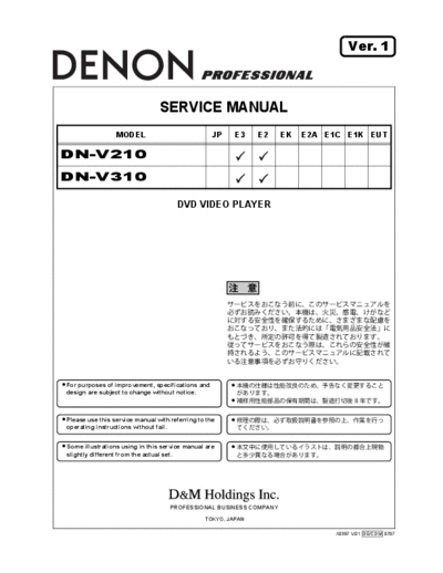
Ver. 1
SERVICE MANUAL
MODEL JP E3 E2 EK E2A E1C E1K EUT
DN-V210
DN-V310
DVD VIDEO PLAYER
For purposes of improvement, specifications and
design are subject to change without notice.
Please use this service manual with referring to the
operating instructions without fail.
Some illustrations using in this service manual are
slightly different from the actual set.
PROFESSIONAL BUSINESS COMPANY
TOKYO, JAPAN
X0357 V.01 DE/CDM 0707
DN-V210/DN-V310
SAFETY PRECAUTIONS
The following check should be performed for the continued protection of the customer and service technician.
LEAKAGE CURRENT CHECK
Before returning the unit to the customer, make sure you make either (1) a leakage current check or (2) a line to chassis
resistance check. If the leakage current exceeds 0.5 milliamps, or if the resistance from chassis to either side of the power
cord is less than 460 kohms, the unit is defective.
LASER RADIATION
Do not stare into beam or view directly with optical instruments, class 3A laser product.
CAUTION Please heed the points listed below during servicing and inspection.
Heed the cautions! Inspect for safety after servicing!
Spots requiring particular attention when servicing, such as Check that all screws, parts and wires removed or discon-
the cabinet, parts, chassis, etc., have cautions indicated on nected for servicing have been put back in their original posi-
labels or seals. Be sure to heed these cautions and the cau- tions, inspect that no parts around the area that has been
tions indicated in the handling instructions. serviced have been negatively affected, conduct an insulation
check on the external metal connectors and between the
Caution concerning electric shock! blades of the power plug, and otherwise check that safety is
ensured.
(1) An AC voltage is impressed on this set, so touching inter-
nal metal parts when the set is energized could cause
(Insulation check procedure)
electric shock. Take care to avoid electric shock, by for ex-
Unplug the power cord from the power outlet, disconnect the
ample using an isolating transformer and gloves when
antenna, plugs, etc., and turn the power switch on. Using a
servicing while the set is energized, unplugging the power
500V insulation resistance tester, check that the insulation re-
cord when replacing parts, etc.
sistance between the terminals of the power plug and the ex-
(2)There are high voltage parts inside. Handle with extra care ternally exposed metal parts (antenna terminal, headphones
when the set is energized. terminal, microphone terminal, input terminal, etc.) is 1M or
greater. If it is less, the set must be inspected and repaired.
Caution concerning disassembly and assembly!
Though great care is taken when manufacturing parts from
sheet metal, there may in some rare cases be burrs on the
edges of parts which could cause injury if fingers are moved CAUTION Concerning important safety parts
across them. Use gloves to protect your hands.
Many of the electric and structural parts used in the set have
Only use designated parts! special safety properties. In most cases these properties are
difficult to distinguish by sight, and using replacement parts
The set's parts have specific safety properties (fire resis- with higher ratings (rated power and withstand voltage) does
tance, voltage resistance, etc.). For replacement parts, be not necessarily guarantee that safety performance will be pre-
sure to use parts which have the same properties. In particu- served. Parts with safety properties are indicated as shown
lar, for the important safety parts that are marked ! on wiring below on the wiring diagrams and parts lists is this service
diagrams and parts lists, be sure to use the designated parts. manual. Be sure to replace them with parts with the designat-
ed part number.
Be sure to mount parts and arrange the
wires as they were originally! (1) Schematic diagrams ... Indicated by the ! mark.
For safety reasons, some parts use tape, tubes or other insu- (2) Parts lists ... Indicated by the ! mark.
lating materials, and some parts are mounted away from the
Using parts other than the designated parts
surface of printed circuit boards. Care is also taken with the
could result in electric shock, fires or other
positions of the wires inside and clamps are used to keep
dangerous situations.
wires away from heating and high voltage parts, so be sure to
set everything back as it was originally.
2
DN-V210/DN-V310
BLOCK DIAGRAM
3
DN-V210/DN-V310
SEMICONDUCTORS
Only major semiconductors are shown, general semiconductors etc. are omitted to list.
IC's
ZR36888HLCG (IC10)
Pin Functions Dir. Description
1 GPCI/O[52] I/O General purpose input/output, monitored/controlled by the CPU or DSP SW
DVDVALID I AV data valid input for FE by-pass. Programmable polarity
FCUIF[35] O Flash card interface unit output signal
2 GPCI/O[53] I/O General purpose input/output, monitored/controlled by the CPU or DSP SW
DVDSOS I AV start of sector indication input for FE by-pass. Programmable polarity
AOUT[4] O Serial output of digital stereo audio
3 GPCI/O[54] I/O General purpose input/output, monitored/controlled by the CPU or DSP SW
FCUIF[30] I/O Flash card interface unit input/output signal
4 GPCI/O[55] I/O General purpose input/output, monitored/controlled by the CPU or DSP SW
FCUIF[31] I/O Flash card interface unit input/output signal
5 GPCI/O[56] I/O General purpose input/output, monitored/controlled by the CPU or DSP SW
DVDREQ O AV data request output for FE by-pass. Programmable polarity
6 GPCI/O[57] I/O General purpose input/output, monitored/controlled by the CPU or DSP SW
FCUIF[36] I/O Flash card interface unit input/output signal
7 GPCI/O[58] I/O General purpose input/output, monitored/controlled by the CPU or DSP SW
FCUIF[33] I/O Flash card interface unit input/output signal
8 SSCCLK I SSC clock input signal
GPCI/O[59] I/O General purpose input/output, monitored/controlled by the CPU or V8 SW
FGPCI/O[4] I/O General purpose input/output, monitored/controlled by the V8 SW
9 SSCTXD O SSC data output signal
GPCI/O[60] I/O General purpose input/output, monitored/controlled by the CPU or V8 SW
FGPCI/O[5] I/O General purpose input/output, monitored/controlled by the V8 SW
10 SSCRXD I SSC data input
GPCI/O[17] I/O General purpose input/output, monitored/controlled by the CPU or DSP or V8 SW
4
DN-V210/DN-V310
Pin Functions Dir. Description
FGPCI/O[0] I/O General purpose input/output, monitored/controlled by the V8 SW
PM[5] O Probe mux data output
11 MEMCS[1]# O PNVM/SRAM chip select (active low) output
GPCI/O[18] I/O General purpose input/output, monitored/controlled by the CPU or DSP SW
FCUIF[29] O Flash card interface unit output signal
MEMLSB O PNVM/SRAM address I.s. byte select output
12 VDDP S 3.3 V Digital periphery power supply
13, 14 MEMAD[15,16] O PNVM/SRAM address bus outputs
FCUIF[45,46] O Flash card interface unit output signal
SYSIND[1,0] I General purpose system configuration indication input. Level sampled during RESET
15 MEMAD[14] O PNVM/SRAM address bus output
FCUIF[44] O Flash card interface unit output signal
PLLUBYP I PLLu by-pass selection input. Level sampled during RESET. In normal operation the pin
must be low during RESET
16 MEMAD[13] O PNVM/SRAM address bus output
FCUIF[43] O Flash card interface unit output signal
17 MEMAD[12] O PNVM/SRAM address bus output
FCUIF[42] O Flash card interface unit output signal
PHSPLLBYP I Processing HS PLL by-pass selection input. Level sampled during RESET. In normal oper-
ation the pin must be low during RESET
18 MEMAD[15] I/O PNVM/SRAM bi-directional data bus
FCUIF[28] I/O Flash card interface unit input/output signal
19 MEMAD[11] O PNVM/SRAM address bus output
FCUIF[41] O Flash card interface unit output signal
PDIV2BYP I PDIV2 by-pass selection input. Level sampled during RESET. In normal operation the pin
must be low during RESET
20 MEMDA[7] I/O PNVM/SRAM bi-directional data bus
FCUIF[9] I/O Flash card interface unit input/output signals
21 GNDP S Digital periphery ground of 3.3 V supply
22 MEMAD[10] O PNVM/SRAM address bus output
FCUIF[20] O Flash card interface unit output signal
TESTMODE I Operational mode selection. Level sampled during RESET. In normal operation the pin
must be low during RESET
23 MEMAD[14] I/O PNVM/SRAM bi-directional data bus
FCUIF[27] I/O Flash card interface unit input/output signal
24 MEMAD[9] O PNVM/SRAM address bus output
FCUIF[19] O Flash card interface unit output signal
PLLEBYP I PLLe by-pass selection input. Level sampled during RESET. In normal operation the pin
must be low during RESET
25 MEMAD[6] I/O PNVM/SRAM bi-directional data bus
FCUIF[8] I/O Flash card interface unit input/output signal
26 MEMAD[8] O PNVM/SRAM address bus output
FCUIF[18] O Flash card interface unit output signal
27 MEMAD[13] I/O PNVM/SRAM bi-directional data bus
FCUIF[26] I/O Flash card interface unit input/output signal
28 MEMAD[5] I/O PNVM/SRAM bi-directional data bus
FCUIF[7] I/O Flash card interface unit input/output signal
29 MEDAD[20] O PNVM/SRAM address bus output
MEMCS[2]# O PNVM/SRAM chip select (active low) output
GPCI/O[19] I/O General purpose input/output, monitored/controlled by the CPU or DSP SW
FCUIF[50] O Flash card interface unit output signal
MEMMSB O PNVM/SRAM address m.s. byte select output
30 VDDP S 3.3 V Digital periphery power supply
31 MEMAD[12] I/O PNVM/SRAM bi-directional data bus
FCUIF[25] I/O Flash card interface unit input/output signal
32 MEMWR# O PNVM/SRAM write enable (active low) output
FCUIF[0] O Flash card interface unit output signal
33 MEMAD[4] I/O PNVM/SRAM bi-directional data bus
FCUIF[6] I/O Flash card interface unit input/output signal
34 VDDC S 1.8 V Digital core power supply
35 MEMAD[11] I/O PNVM/SRAM bi-directional data bus
FCUIF[24] I/O Flash card interface unit input/output signals
36 MEMAD[3] O PNVM/SRAM bi-directional data bus
FCUIF[5] O Flash card interface unit output signal
37 MEMAD[19] O PNVM/SRAM address bus output
FCUIF[49] O Flash card interface unit output signal
5
DN-V210/DN-V310
Pin Functions Dir. Description
PLLABYP I PLLA by-pass selection input. Level sampled during RESET. In normal operation the pin
must be low during RESET
38 GNDC S Digital core ground of 1.8 V supply
39 MEMAD[10] I/O PNVM/SRAM bi-directional data bus
FCUIF[23] I/O Flash card interface unit input/output signal
40 MEMAD[18] O PNVM/SRAM address bus output
FCUIF[48] O Flash card interface unit output signal
BYTEMODE I Byte access mode selection input. Level sampled during RESET
41 GNDP S Digital periphery ground of 3.3 V supply
42 MEMAD[2] I/O PNVM/SRAM bi-directional data bus
FCUIF[4] I/O Flash card interface unit input/output signal
43 MEMAD[17] O PNVM/SRAM address bus output
FCUIF[47] O Flash card interface unit output signal
SYSIND[2] I General purpose system configuration indication input. Level sampled during RESET
44 MEMDA[9] I/O PNVM/SRAM bi-directional data bus
MEMAD[21] O PNVM/SRAM address bus output
FCUIF[22] I/O Flash card interface unit input/output signal
45 MEMAD[7] O PNVM/SRAM address bus output
FCUIF[17] O Flash card interface unit output signal
FLASHCFG I External flash memory configuration indication input. Level sampled during RESET
46 MEMDA[1] I/O PNVM/SRAM bi-directional data bus
FCUIF[3] I/O Flash card interface unit input/output signal
47 MEMAD[6] O PNVM/SRAM address bus output
FCUIF[16] O Flash card interface unit output signal
48 MEMDA[8] I/O PNVM/SRAM bi-directional data bus
MEMAD[20] O PNVM/SRAM address bus output
FCUIF[21] I/O Flash card interface unit input/output signal
49 MEMAD[5] O PNVM/SRAM address bus output
FCUIF[15] O Flash card interface unit output signal
50 VDDP S 3.3 V Digital periphery power supply
51 MEMDA[0] I/O PNVM/SRAM bi-directional data bus
FCUIF[2] I/O Flash card interface unit input/output signal
52 MEMAD[4] I/O PNVM/SRAM address bus output
FCUIF[14] O Flash card interface unit output signal
53 MEMRD# O PNVM/SRAM read enable (active low) output
FCUIF[1] O Flash card interface unit output signal
54, 55 MEMAD[3,2] O PNVM/SRAM address bus output
FCUIF[13,12] O Flash card interface unit output signal
56 MEMCS[0]# O PNVM/SRAM chip select (active low) output
FCUIF[38] O Flash card interface unit output signal
57,58 MEMAD[1,0] O PNVM/SRAM address bus output
FCUIF[11,10] O Flash card interface unit output signal
BOOTSEL[2,1] I CPU SW boot (and execute) source selection. Levels sampled during RESET
59 GNDP S Digital periphery ground of 3.3 V supply
60 VDD-IP S 3.3 V periphery reference voltage
61 VDDP S 3.3 V Digital periphery power supply
62 GPCI/O[61] I/O General purpose input/output, monitored/controlled by the CPU or V8 SW
FGPCI/O[6] I/O General purpose input/output, monitored/controlled by the CPU or V8 SW
63 FGPCI/O[62] I/O General purpose input/output, monitored/controlled by the CPU or V8 SW
FGPCI/O[7] I/O General purpose input/output, monitored/controlled by the V8 SW
64 RAMCKE O Clock enable signal to the SDRAM (for power down)
GPCI/O[63] I/O General purpose input/output, monitored/controlled by the CPU or DSP SW
65 VDDUSB S 3.3 V USB power supply
66 USBDP I/O USB data positive signal
67 USBDN I/O USB data negative signal
68 GNDUSB S Ground for USB 3.3 V supply
69-73 RAMADD[4,3,5,2,6] O SDRAM address bus output
74 VDDP S 3.3 V Digital periphery power supply
75-77 RAMADD[1,7,0] O SDRAM address bus output
78 GNDP S Digital periphery ground of 3.3 V supply
79 RAMADD[8] O SDRAM address bus output
80 VDDC S 1.8 V Digital core power supply
81 RAMADD[10] O SDRAM address bus output
82 GNDC S Digital core ground of 1.8 V supply
83 RAMADD[9] O SDRAM address bus output
84 VDDP S 3.3 V Digital periphery power supply
85 RAMADD[11] O SDRAM address bus output
6
DN-V210/DN-V310
Pin Functions Dir. Description
86 RAMCS[0]# O SDRAM chip select (active low)
RAMBA[1] O SDRAM bank select output
87 RAMBA[0] O SDRAM bank select output
88 GNDP S Digital periphery ground of 3.3 V supply
89 RAMCS[1]# O SDRAM chip select (active low) output
90 RAMRAS# O SDRAM row select (active low) output
91 RAMCAS# O SDRAM column select (active low) output
92 VDDP S 3.3 V Digital periphery power supply
93 RAMWE# O SDRAM write enable (active low) output
94 RAMDQM O SDRAM data masking (active high) output
95 GNDPCLK S Digital ground of filtered 3.3 V supply for PCLK
96 PCLK O SDRAM clock output (same as internal processing clock)
97 VDDPCLK S 3.3 V filtered digital power supply for PCLK
98 RAMDAT[8] I/O SDRAM bi-directional data bus
99 GNDP S Digital periphery ground of 3.3 V supply
100-102 RAMDAT[7,9,6,] I/O SDRAM bi-directional data bus
103 VDDP S 3.3 V Digital periphery power supply
104-106 RAMDAT[10,5,11] I/O SDRAM bi-directional data bus
107 GNDP S Digital periphery ground of 3.3 V supply
108 RAMDAT[4] I/O SDRAM bi-directional data bus
109 VDDC S 1.8 V Digital core power supply
110 RAMDAT[12] I/O SDRAM bi-directional data bus
111 GNDC S Digital core ground of 1.8 V supply
112 RAMDAT[3] I/O SDRAM bi-directional data bus
113 VDDP S 3.3 V Digital periphery power supply
114-116 RAMDAT[13,2,14] I/O SDRAM bi-directional data bus
117 GNDP S Digital periphery ground of 3.3 V supply
118-120 RAMDAT[1,15,0] I/O SDRAM bi-directional data bus
121 VDDP S 3.3 V Digital periphery power supply
122 GPCI/O[20] I/O General purpose input/output, monitored/controlled by the CPU or DSP SW
CPUNMI I CPU non-maskable interrupt input
RAMCKE O Clock enable signal to the SDRAM (for power down)
AIN[4] I Serial output of digital stereo audio
PM[0] O Probe mux data output
123 GNDP S Digital periphery ground of 3.3 V supply
124 ICGPCI/O[0] I/O General purpose input/output, monitored/controlled by the CPU or DSP SW. When input,
the pin can be used as general purpose external interrupt to the CPU
AOUT[3] O Serial output of digital stereo audio
ADPWMP[0] O Class D audio channel 0 output, positive signal
ADPWMP[6] O Class D audio channel 6 output, positive signal
PM[1] O Probe mux data output
125 IDGPCI/O[0] I/O General purpose input/output, monitored/controlled by the CPU or DSP SW. When input,
the pin can be used as general purpose external interrupt to the DSP
S/PDIFIN[5] I S/PDIF receiver input for detail coded or reconstructed audio data
ADPWMP[6] O Class D audio channel 6 output, negative signal
PM[2] O Probe mux data output
126 GPCI/O[64] I/O General purpose input/output, monitored/controlled by the CPU or DSP SW
S/PDIFOUT O S/PDIF transmitter output for detail coded or reconstructed audio data
ADPWMP[5] O Class D audio channel 5 output, positive signal
PM[3] O Probe mux data output
127 ADPWMN[5] O Class D audio channel 5 output, negative signal
ADPWMN[0] O Class D audio channel 0 output, negative signal
GPCI/O[21] I/O General purpose input/output, monitored/controlled by the CPU or DSP SW
AOUT[2] O Serial output of digital stereo audio
PM[4] O Probe mux data output
128 ADPWMN[4] O Class D audio channel 4 output, positive signal
ADPWMN[1] O Class D audio channel 1 output, positive signal
GPCI/O[22] I/O General purpose input/output, monitored/controlled by the CPU or DSP SW.
AOUT[1] O Serial output of digital stereo audio
PM[5] O Probe mux data output
129 AOUT[0] O Serial output of digital stereo audio
ADPWMN[1] O Class D audio channel 0 output, negative signal
130 GPAI/O I/O General purpose input/output, monitored/controlled by the ADP SW.
AOUT[3] O Serial output of digital stereo audio
GPCI/O[65] I/O General purpose input/output, monitored/controlled by the CPU SW.
S/PDIFIN[1] I S/PDIF receiver input for detail coded or reconstructed audio data
AIN[2] I Serial input of digital stereo audio
7
DN-V210/DN-V310
Pin Functions Dir. Description
ADPWMN[2] O Class D audio channel 2 output, negative signal
PM[7] O Probe mux data output
131 ALRCLK O Digital audio left/right select output for the audio port. Square wave, at the sampling fre-
quency. Programmable polarity
GPCI/O[66] I/O General purpose input/output, monitored/controlled by the CPU or DSP SW
AUTO[4] O Serial outputs of digital stereo audio
132 ABCLK O Digital audio bit-clock output. Data on AOUT and AIN is output or latched, respectively, with
the rising or falling (programmable) edge of this clock
GPCI/O[67] I/O General purpose input/output, monitored/controlled by the CPU or DSP SW
133 GNDP-A2 S Digital ground of filtered 3.3 V supply for AMCLK
134 AMCLK I/O Audio Master Clock input/output. 128, 192, 256 or 384 times the sampling frequency (pro-
grammable)
135 VDDP-A2 S 3.3V filtered digital power supply for AMCLK
136 AIN[1] I Serial input of digital stereo audio
GPCI/O[23] I/O General purpose input/output, monitored/controlled by the CPU or DSP SW
ADPWMP[2] O Class D audio channel 2 output, positive signal
PM[8] O Probe mux data output
137 VSYNC# O SD digital video vertical sync output signal
HDFI I HD digital video index signal
GPCI/O[24] I/O General purpose input/output, monitored/controlled by the CPU or DSP SW
DACTEST[9] I DACs rest input
PM[9] O Probe mux data output
138 HSYNC# O SD digital video horizontal sync output signal
HDHS I HD digital video horizontal sync output signal
GPCI/O[25] I/O General purpose input/output, monitored/controlled by the CPU or DSP SW
DACTEST[8] I DACs rest input
PM[10] O Probe mux data output
139 GNDP S Digital periphery ground of 3.3 V supply
140 VCLKx2 I/O Digital video clock input/output. 27 MHz (for SD interlaced) or 54 MHz (for SD progressive)
or 135 MHz (for HD to external 177, output only)
COSYNC O Composite sync output. Active only when component analog output is selected
ICGPCI/O[1] I/O General purpose input/output, monitored/controlled by the CPU or DSP SW. When input,
the pin can be used as general purpose external interrupt to the CPU
ADPWMN[2] O Class D audio channel 2 output, negative signal
DACTEST[10] I DACs rest input
PM[11] O Probe mux data output
141 VDDP S 3.3 V Digital periphery power supply
142 VID[7] O Digital 4:2:2 video luma/chroma input/output, interleaved U, Y, V, Y
GPCI/O[26] I/O General purpose input/output, monitored/controlled by the CPU or DSP SW
ADPWMP[3] O Class D audio channel 3 output, positive signal
DACTEST[7] I DACs rest input
143 VID[6] I/O Digital 4:2:2 video luma/chroma input/output, interleaved U, Y, V, Y
ICGPCI/O[2] I/O General purpose input/output, monitored/controlled by the CPU or DSP SW. When input,
the pin can be used as general purpose external interrupt to the CPU
ADPWMN[3] O Class D audio channel 3 output, negative signal
DACTEST[6] I DACs rest input
144 VID[5] I/O Digital 4:2:2 video luma/chroma input/output, interleaved U, Y, V, Y
IDGPCI/O[1] I/O General purpose input/output, monitored/controlled by the CPU or DSP SW. When input,
the pin can be used as general purpose external interrupt to the DSP
ADPWMN[4] O Class D audio channel 4 output, negative signal
DACTEST[5] I DACs rest input
145 VID[4] I/O Digital 4:2:2 video luma/chroma input/output, interleaved U, Y, V, Y
GPCI/O[27] I/O General purpose input/output, monitored/controlled by the CPU or DSP SW
ADPWMN[4] O Class D audio channel 4 output, negative signal
DACTEST[4] I DACs rest input
- GNDP S Digital periphery ground of 3.3 V supply
146 GNDC S Digital core ground of 1.8 V supply
147 VDDC S 1.8 V Digital core power supply
- VDDP S 3.3 V Digital periphery supply
148 VID[3] I/O Digital 4:2:2 video luma/chroma input/output, interleaved U, Y, V, Y
GPCI/O[28] I/O General purpose input/output, monitored/controlled by the CPU or DSP SW
ADPWMN[5] O Class D audio channel 5 output, negative signal
DACTEST[3] I DACs rest input
PM[6] O Probe mux data output
149 VID[2] I/O Digital 4:2:2 video luma/chroma input/output, interleaved U, Y, V, Y
GPCI/O[29] I/O General purpose input/output, monitored/controlled by the CPU or DSP SW
ADPWMN[5] O Class D audio channel 5 output, negative signal
DACTEST[2] I DACs rest input
8
DN-V210/DN-V310
Pin Functions Dir. Description
PM[12] O Probe mux data output
150 VID[1] I/O Digital 4:2:2 video luma/chroma input/output, interleaved U, Y, V, Y
GPCI/O[30] I/O General purpose input/output, monitored/controlled by the CPU or DSP SW
ADPWMN[6] O Class D audio channel 6 output, positive signal
DACTEST[1] I DACs rest input
PM[13] O Probe mux data output
151 VID[0] I/O Digital 4:2:2 video luma/chroma input/output, interleaved U, Y, V, Y
ICGPCI/O[3] I/O General purpose input/output, monitored/controlled by the CPU or DSP SW. When input,
the pin can be used as general purpose external interrupt to the CPU
ADPWMN[6] O Class D audio channel 6 output, negative signal
DACTEST[0] I DACs rest input
PM[14] O Probe mux data output
152 GPCI/O[31] I/O General purpose input/output, monitored/controlled by the CPU or DSP SW
ADPWMN[7] O Class D audio channel 7 output, positive signal
AOUT[4] O Serial output of digital stereo audio
PMCLK O Probe mux data output
153 IDGPCI/O[2] I/O General purpose input/output, monitored/controlled by the CPU or DSP SW. When input,
the pin can be used as general purpose external interrupt to the DSP
AOUT[5] O Serial output of digital stereo audio
ADPWMN[7] O Class D audio channel 7 output, negative signal
154 VDDP S 3.3 V Digital periphery power supply
155 GNDP S Digital periphery ground of 3.3 V supply
156 GNDA S Ground plane of internal PLL circuit
157 RESET# ID Reset input (active low)
158 VDDA S 1.8 V Power supply for internal PLL circuit
159 XO AO Output to a crystal that is connected to GCLKP. If a crystal is not used at GCLKP, XO must
be left not connected
160 GCLKP ID 27.000MHz clock generator or crystal input for the PLL
161 AHVDD S 1.8 V Power supply for the HD PLL
162 AHGND S Ground for the 1.8V HD PLL power supply
163 AGNDP S Ground for the 3.3V HD unit power supply
164 HDTXCN O HDMI clock negative output signal
165 HDTXCP O HDMI clock positive output signal
166 AVDDP S 3.3V Power supply for the HD unit
167 HDTXDN0 O HDMI data channel 0 negative output signal
168 HDTXDP0 O HDMI data channel 0 positive output signal
169 AGNDP S Ground for the 3.3V HD unit power supply
170 HDTXDN1 O HDMI data channel 1 negative output signal
171 HDTXDP1 O HDMI data channel 1 positive output signal
172 AVDDP S 3.3V Power supply for the HD unit
173 HDTXDN2 O HDMI data channel 2 negative output signal
174 HDTXDP2 O HDMI data channel 2 positive output signal
175 AGNDP S Ground for the 3.3V HD unit power supply
176 HDCSET AI/O Resistive load for output current setting
177 AGNDC S Ground for 1.8V HD unit power supply
179, 180 GNDDACD S Ground for the video DACs 3.3 V analog power supply
181 CVBS (DAC 6) Analog CVBS (SD only) video output
182 VDDDACD S Ground for video DACs 3.3 V analog power supply
183 CVBS/C/Y (DAC 5) AO Analog video output that can be selected to be CVBS (SD only), C (SD only) or Y (SD only).
The selection is independent the specific selection of the other four DACs
184 CVBS/G/Y (DAC 4) AO Analog video output that can be selected to be CVBS (SD only), or G/Y (SD or HD). The
selection is independent of the specific selection of the other four DACs. The selection
between G and Y depends also on DACs 1 and 2 selections
185 VDDDAC S 3.3 V Analog power supply for the video DACs
186 CVBS/C/Y (DAC 3) AO Analog video output that can be selected to be CVBS (SD only), C (SD only) or Y (SD only).
The selection is independent of the specific selection of the other four DACs
187 Y/R/V/C (DAC 2) AO Analog video output that can be selected to be Y (SD only), or R/V (SD or HD) or C (SD
only). The selection is independent of the specific selection of the other four DACs. The
selection between R and V depends also on DACs 1 and 4 selections
188 VDDDAC S 3.3 V Analog power supply for the video DACs
189 C/B/U (DAC 1) AO Analog video output that can be selected to be C (SD only), or B/U (SD or HD). The selec-
tion is independent of the specific selection of the other four DACs. The selection between
B and U depends also on DACs 2 and 4 selections
190 RSET AI/O Resistive load for gain adjustment of the DACs
191 GNDDACP S Ground for the video DACs 3.3 V analog power supply
192 GNDDABS2 S Common Ground for the video and SERVO DACs
193 RFINP AI RF positive input signal (differential input) // RF input signal (single ended)
194 RFINN AI RF negative input signal (differential input) // RF reference input signal
9
DN-V210/DN-V310
Pin Functions Dir. Description
195 ADCIN[G] AI ADC input signal (e.g. from OPU)
196 ADCIN[A] AI ADC input signal (e.g. from OPU)
197 VDDAFE S Analog AFE 3.3 V supply
198 ADCIN[B] AI ADC input signal (e.g. from OPU)
199 VDDSAFE S Analog AFE 3.3 V supply shield
200 VDDAFE S Analog AFE 3.3 V supply
201 ADCIN[C] AI ADC input signal (e.g. from OPU)
202 ADCIN[H] AI ADC input signal (e.g. from OPU)
203, 204 ADCIN[D,J] AI ADC input signals (e.g. from OPU)
205 GNDADC S Analog ADC (AFE) ground of 3.3 V supply
206-208 ADCIN[E,K,F] AI ADC input signals (e.g. from OPU)
209 OPUREF AO OPU reference voltage output
210 BGCAP AI/O Capacitive load for internal band-gap voltage generation
211 RESLOAD AI/O Resistive load for internal reference voltage generation
212 CDMD AI CD LASER monitor diode input
213 DVDMD AI DVD LASER monitor diode input
214 CDLD AO CD LASER diode drive output
215 DVDLD AO DVD LASER diode drive output
216 GNDAFER AI AFE analog reference voltage ground
217 GNDADC S Analog ADC (AFE) ground of 3.3 V supply
218 VDDC S 1.8 V Digital core power supply
219 GPCI/O[32] I/O General purpose input/output, monitored/controlled by the CPU or DSP SW
FCUIF[32] I/O Flash card interface unit output signal
220 GNDC S Digital core ground of 1.8 V supply
221 ICGPCI/O[4] I/O General purpose input/output, monitored/controlled by the CPU or DSP SW. When input,
the pin can be used as general purpose external interrupt to the CPU
FCUIF[37] O Flash card interface unit output signal
S/PDIFIN[4] I S/PDIF receiver input for detail coded or reconstructed audio data
222 ICGPCI/O[5] I/O General purpose input/output, monitored/controlled by the CPU or DSP SW. When input,
the pin can be used as general purpose external interrupt to the CPU
FCUIF[33] O Flash card interface unit output signal
S/PDIFIN[2] I S/PDIF receiver input for detail coded or reconstructed audio data
223 VDDP S 3.3 V Digital periphery power supply
224 IDGPCI/O[3] I/O General purpose input/output, monitored/controlled by the CPU or DSP SW. When input,
the pin can be used as general purpose external interrupt to the DSP
FCUIF[36] I/O Flash card interface unit input/output signal
225 GNDP S Digital periphery ground of 3.3 V supply
226 ICGPCI/O[6] I/O General purpose input/output, monitored/controlled by the CPU or DSP SW. When input,
the pin can be used as general purpose external interrupt to the CPU
FCUIF[30] I/O Flash card interface unit input/output signal
227 ICGPCI/O[7] I/O General purpose input/output, monitored/controlled by the CPU or DSP SW. When input,
the pin can be used as general purpose external interrupt to the CPU
FCUIF[35] I/O Flash card interface unit input/output signal
228 VDD-IP S 3.3 V periphery reference voltage
229 ICGPCI/O[6] I/O General purpose input/output, monitored/controlled by the CPU or DSP SW. When input,
the pin can be used as general purpose external interrupt to the DSP
FCUIF[31] I/O Flash card interface unit input/output signal
NRZCLK I NZR clock input for AFE and DRC by-pass
230 IDGPCI/O[7] I/O General purpose input/output, monitored/controlled by the CPU or DSP SW. When input,
the pin can be used as general purpose external interrupt to the DSP
FCUIF[34] I/O Flash card interface unit input/output signal
S/PDIFOUT O S/PDIF output for detail coded or reconstructed audio data
231 PWMCO[2] O PWM4 output signal
GPCI/O[43] I/O General purpose input/output, monitored/controlled by the CPU or DSP SW
232 PWMCO[3] O PWM5 output signal
GPCI/O[44] I/O General purpose input/output, monitored/controlled by the CPU or DSP or V8 SW
FGPCI/O[1] I/O General purpose input/output, monitored/controlled by the V8 SW
233 GNDPWMS S SERVO PWMs ground of 3.3V supply
234 PWMCO[4] O PWM6 output signal
GPCI/O[45] I/O General purpose input/output, monitored/controlled by the CPU or DSP SW
RFDAT[2] I RF channel sample data input for RF by-pass
235 VDDPWMS S 3.3 V SERVO PWM power supply
236 PWMCO[5] O PWM7 output signal
GPCI/O[46] I/O General purpose input/output, monitored/controlled by the CPU or DSP SW
237 PWMCO[6] O PWM8 output signal
IDGPCI/O[4] I/O General purpose input/output, monitored/controlled by the CPU or DSP SW. When input,
the pin can be used as general purpose external interrupt to the DSP
238 PWMCO[0] O PWM2 output signal
10
DN-V210/DN-V310
Pin Functions Dir. Description
GPCI/O[41] I/O General purpose input/output, monitored/controlled by the CPU or DSP SW
239 DUPRD0 I First debug UART data input
GPCI/O[35] I/O General purpose input/output, monitored/controlled by the CPU or DSP SW
240 DUPTD0 I First debug UART data input
GPCI/O[36] I/O General purpose input/output, monitored/controlled by the CPU or DSP SW
241 DUPRD1 I Second debug UART data input
GPCI/O[37] I/O General purpose input/output, monitored/controlled by the CPU or DSP SW
242 DUPTD1 O Second debug UART data input
GPCI/O[38] I/O General purpose input/output, monitored/controlled by the CPU or DSP SW
243 FCUIF[37] I/O Flash card interface unit input/output signal
GPCI/O[39] I/O General purpose input/output, monitored/controlled by the CPU or DSP SW
244 GPCI/O[40] I/O General purpose input/output, monitored/controlled by the CPU or DSP SW
DVDDAT[0] I AV data input for FE by-pass
245 VDDP S 3.3 V Digital periphery power supply
246 GPCI/O[42] I/O General purpose input/output, monitored/controlled by the CPU or DSP SW
DVDDAT[1] I AV data input for FE by-pass
247 FCUIF[34] I/O Flash card interface unit input/output signal
GPCI/O[33] I/O General purpose input/output, monitored/controlled by the CPU or DSP SW
DVDERR I AV error indication input for FE by-pass. Programmable polarity
248 FCUIF[32] I/O Flash card interface unit output signal
GPCI/O[34] I/O General purpose input/output, monitored/controlled by the CPU or DSP SW
249 IDGPCI/O[5] I/O General purpose input/output, monitored/controlled by the CPU or DSP SW. When input,
the pin can be used as general purpose external interrupt to the DSP
DVDDAT[2] I AV data input for FE by-pass
250 GPCI/O[48] I/O General purpose input/output, monitored/controlled by the CPU or DSP SW
DVDDAT[3] I AV data input for FE by-pass
251 GPCI/O[49] I/O General purpose input/output, monitored/controlled by the CPU or DSP SW
DVDDAT[4] I AV data input for FE by-pass
252 GPCI/O[50] I/O General purpose input/output, monitored/controlled by the CPU or DSP SW
DVDDAT[5] I AV data input for FE by-pass
253 GPCI/O[51] I/O General purpose input/output, monitored/controlled by the CPU or DSP SW
DVDDAT[6] I AV data input for FE by-pass
254 SSCCLK I SSC clock input signal
GPCI/O[47] I/O General purpose input/output, monitored/controlled by the CPU or DSP or V8 SW
FGPCI/O[2] I/O General purpose input/output, monitored/controlled by the V8 SW
DVDDAT[7] I AV data input for FE by-pass
255 SSCTXD O SSC clock input signal
GPCI/O[16] I/O General purpose input/output, monitored/controlled by the CPU or DSP or V8 SW
FGPCI/O[3] I/O General purpose input/output, monitored/controlled by the V8 SW
DVDSTRB I AV bit strobe input. Programmable polarity
256 GNDP S Digital periphery ground of 3.3 V supply
M29W160ET-70N (IC11)
A15 1 48 A16
A14 BYTE
A13 VSS
A12 DQ15A◦ Jabse Service Manual Search 2026 ◦ Jabse Pravopis ◦ onTap.bg ◦ Other service manual resources online : Fixya ◦ eServiceinfo