Service Manuals, User Guides, Schematic Diagrams or docs for : DENON AM FM Stereo Tuner AM FM Stereo Tuner Denon - TU-1800DAB Схема TU-1800DAB

<< Back | Home

Most service manuals and schematics are PDF files, so You will need Adobre Acrobat Reader to view : Acrobat Download Some of the files are DjVu format. Readers and resources available here : DjVu Resources
For the compressed files, most common are zip and rar. Please, extract files with Your favorite compression software ( WinZip, WinRAR ... ) before viewing. If a document has multiple parts, You should download all, before extracting.
Good luck. Repair on Your own risk. Make sure You know what You are doing.


Image preview - the first page of the document
Схема TU-1800DAB


>> Download Схема TU-1800DAB documenatation <<

Text preview - extract from the document
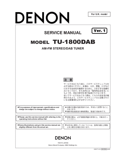
                                                                             For U.K. model


                                                                               Ver. 1
                               SERVICE MANUAL

              MODEL                      TU-1800DAB
                            AM-FM STEREO/DAB TUNER


For purposes of improvement, specifications and
design are subject to change without notice.


Please use this service manual with referring to the
operating instructions without fail.


Some illustrations using in this service manual are
slightly different from the actual set.


                                                TOKYO JAPAN
                                    Denon Brand Company, D&M Holdings Inc.

                                                                               X0237 V.01 DE/CDM 0507
                                                                                                            TU-1800DAB


SAFETY PRECAUTIONS
The following check should be performed for the continued protection of the customer and service technician.

LEAKAGE CURRENT CHECK
Before returning the unit to the customer, make sure you make either (1) a leakage current check or (2) a line to chassis
resistance check. If the leakage current exceeds 0.5 milliamps, or if the resistance from chassis to either side of the
power cord is less than 460 kohms, the unit is defective.


                                                            2
                     TU-1800DAB


LEVEL DIAGRAMS


                 3
                     TU-1800DAB
BLOCK DIAGRAMS


                 4
                                                                                         TU-1800DAB


SEMICONDUCTORS
 Only major semiconductors are shown, general semiconductors etc. are omitted to list.


1. IC's

MB90F352C (IC300)


                                                              5
                                                                          TU-1800DAB

MB90F352C Terminal Function
   Pin No.   Pin Name               I/O   Function
     1       Avss                         Vss
     2       AVRH                         Vcc
     3       P62/AN2/PPG4(5)         I    key1
     4       P63/AN3/PPG6(7)         I    key2
     5       P64/AN4/PPG8(9)         I    encoder_a
     6       P65/AN5/PPGA(B)         I    encoder_b
     7       P66/AN6/PPGC(D)        O     FLT_RESET
     8       P67/AN7/PPGE(F)        O     FLT_SELECT
     9       P50/AN8/SIN2           O     FLT_CLOCK
     10      P51/AN9/SOT2           O     FLT_DATA
     11      P52/AN10/SCK2          O     RDI_SELECT
     12      P53/AN11/TIN3          O
     13      P54/AN12/TOT3          O     LED_STANDBY
     14      P55/AN13               O     LED_STEREO
     15      P56/AN14               O     LED_SECONDARY
     16      P42/IN6/RX1/INT9R      O     LED_TUNED
     17      P43/INT7/TX1           O     LED_RDS
     18      Vss                          GND
     19      P40/X0A
     20      P41/X1A
     21      MD2                          MICOM UPGRADE
     22      MD1                          MICOM UPGRADE
     23      MD0                          MICOM UPGRADE
     24      P00/AD00/INT8          O     DAB_I2C_CLOCK
     25      P01/AD01/INT9          O     DAB_I2C_DATA
     26      P02/AD02/INT10          I    AK4103_DATA_IN
     27      P03/AD03/INT11         O     AK4103_CLOCK
     28      P04/AD04/INT12         O     AK4103_DATA_OUT
     29      P05/AD05/INT13         O     AK4103_SELECT
     30      P06/AD06/INT14          I    POWER_DOWN
     31      P07/AD07/INT15          I    REMOCON
     32      P10/AD08/TIN1          O     POWER_RELAY
     33      P11/AD09/TOT1          O     MAIN_MUTE
     34      P12/AD10/SIN3/INT11R   O     UPGRADE_RX
     35      P13/AD1A/SOT3          O     UPGRADE_TX
     36      P14/AD12/SCK3          O     POWER_DAB
     37      P15/AD13               O
     38      P16/AD14               O     EEPROM_DATA
     39      P17/AD15               O     EEPROM_CLOCK
     40      P20/A16/PPG9(8)        O     DIT_RESET
     41      P21/A17/PPGB(A)        O     FUNCTION_RELAY
     42      P22/A18/PPGD?          O     DAC_RESET
     43      P23/A19/PPGF(E)         I    DAC_MUTE_DETECT_R
     44      P24/A20/IN0             I    DAC_MUTE_DETECT_L
     45      RST
     46      X1                           4MHz
     47      X0                           4MHz
     48      Vss
     49      Vcc
     50      C                            0.1UF/CERAMIC
     51      P25/A21/IN1/ADTG       O     DAC_MUTE
     52      P44/FRCK0              O
     53      P45/FRCK1              O
     54      P30/ALE/IN4            O     DAB_ON
     55      P31/RD/IN5              I    RDS_DATA
     56      P32/WRL/WR/INT10R       I    RDS_CLOCK
     57      P33/WRH                O     PLL_CE
     58      P34/HRQ/OUT4           O     PLL_DATA_OUT(PLL DATA TRANS )
     59      P35/HAK/OUT5           O     PLL_CLOCK
     60      P36/RDY/OUT6            I    PLL_DATA_IN(IF READ)
     61      P37/CLK/OUT7           O     TUNER_MUTE
     62      P60/AN0                 I    TUNER_STEREO
     63      P61/AN1                 I    TUNER_TUNED
     64      Avcc                         VCC


                                                            6
                                                                                                                                                          TU-1800DAB

AK4103A (IC304)


             V1         1                                  24                  U1

             TRANS      2                                  23                  DIF2

             PDN        3                                  22                  DIF1

             MCLK       4                                  21                  DIF0

             SDTI       5                                  20                  TXP

             BICK       6      Top                         19                  TXN
                               View
             LRCK       7                                  18                  VSS

             FS0/CSN    8                                  17                  VDD

             FS1/CDTI   9                                  16                  CKS1

             FS2/CCLK   10                                 15                  CKS0

             FS3/CDTO   11                                 14                  BLS

             C1         12                                 13                  ANS


AK4103A BLOCK DIAGRAM


                                                                                                          TRANS
                                                                                      MCLK
                                                                        CKS0
                                                                CKS1
                               DIF2
                                      DIF1
                                             DIF0


                                                                                                                                                   VDD
                                                                                                                         VSS
                                                                                                    BLS


          BICK                                                                 Prescaler
         LRCK                Audio Serial
                              Interface
          SDTI
                                                                                                                               RS422 Line Driver


           C1
           U1                                                                  Biphase                                                                   TXP

           V1                                                                  Encoder
                                                                                                                                                         TXN
                                                Register
                             MUX


          FS0
          FS1
                                                                       CRCC Generator
          FS2
          FS3
                                                                        Host Serial
                                                                         Interface
                                                                                      CDTI

                                                                                             CDTO
                                                                               CCLK
                                                                  CSN


                                                                                                                        PDN
                                                                                                                  ANS


                                                                       7
                                                                                                                    TU-1800DAB

AK4103A TERMINAL FUNCTION


       No.     Pin Name            I/O                                          Description
        1      V1                    I      Validity Bit Input Pin
        2      TRANS                 I      Audio Routing Mode (Transparent Mode) Pin at Synchronous mode
                                              0: Normal mode, 1: Audio routing mode (transparent mode)
        3      PDN                   I      Power Down & Reset Pin                                   (Pull-up Pin)
                                              When "L", the AK4103A is powered-down, TXP/N pins are "L" and the
                                              control registers are reset to default values.
        4      MCLK                  I      Master Clock Input Pin
        5      SDTI                  I      Audio Serial Data Input Pin
        6      BICK                I/O      Audio Serial Data Clock Input/Output Pin
                                              Serial Clock for SDTI pin which can be configured as an output based on
                                              the DIF2-0 inputs.
        7      LRCK                I/O      Input/Output Channel Clock Pin
                                              Indicates left or right channel, and can be configured as an output based on
                                              the DIF2-0 inputs.
        8      FS0                   I      Sampling Frequency Select 0 Pin at Synchronous mode (Pull-down Pin)
               CSN                   I      Host Interface Chip Select Pin at Asynchronous mode (Pull-down Pin)
               AKMODE                I      AK4112B Mode Pin at Audio routing mode                   (Pull-down Pin)
                                              0: Non-AKM receivers mode, 1: AK4112B mode
        9      FS1                  I       Sampling Frequency Select 1 Pin at Synchronous mode (Pull-down Pin)
               CDTI                 I       Host Interface Data Input Pin at Asynchronous mode (Pull-down Pin)
       10      FS2                  I       Sampling Frequency Select 2 Pin at Synchronous mode (Pull-down Pin)
               CCLK                 I       Host Interface Bit Clock Input Pin at Asynchronous mode (Pull-down Pin)
       11      FS3                  I       Sampling Frequency Select 3 Pin at Synchronous mode (Pull-down Pin)
               CDTO                 O       Host Interface Data Output Pin at Asynchronous mode (Pull-down Pin)
       12      C1                   I       Channel Status Bit Input Pin
       13      ANS                  I       Asynchronous/Synchronous Mode Select Pin                 (Pull-up Pin)
                                              0: Asynchronous mode, 1: Synchronous mode
       14      BLS                 I/O      Block Start Input/Output Pin                             (Pull-down Pin)
                                              In normal mode, the channel status block output is "H" for the first four
                                              bytes. In audio routing mode, the pin is configured as an input. When PDN
                                              pin = "L", BLS pin goes "H" at Normal mode.
       15      CKS0                  I      Clock Mode Select 0 Pin                                  (Pull-up Pin)
       16      CKS1                  I      Clock Mode Select 1 Pin                                  (Pull-down Pin)
       17      VDD                   -      Power Supply Pin, 4.75V5.25V
       18      VSS                   -      Ground Pin, 0V
       19      TXN                   O      Negative Differential Output Pin
       20      TXP                   O      Positive Differential Output Pin
       21      DIF0                  I      Audio Serial Interface Select 0 Pin                      (Pull-down Pin)
       22      DIF1                  I      Audio Serial Interface Select 1 Pin                      (Pull-down Pin)
       23      DIF2                  I      Audio Serial Interface Select 2 Pin                      (Pull-down Pin)
       24      U1                    I      User Data Bit Input Pin for Channel 1                    (Pull-down Pin)
    Notes:
      1. Internal pull-up and pull-down resistors are connected on-chip. The value of the resistors is 43k (typ).
      2. All input pins except internal pull-down/pull-up pins should not be left floating.


                                                                8
                                                                                                                                                                                           TU-1800DAB

BU1924F (IC306)


                                                                                                                                                      560p


                                                                                                                                                                      CMP

             MUX                       100k                                                                                                     (7)                  (8)
                         (4)                                                                                                             VSS3


             270p
                            120k       100k
                                                                                                        8th Switched
                                                                                                        capacitor filter

                                                                                                                                                             comparator
                                                                anti-aliasing
             Vref        (3)                                        filter


                                                                                                                                                                             (16) RCLK
     2.2 F

                  VDD1   (5)

              1               Analog
                            Power supply                                                                                                                                           QUAL
                                                                                                                                                                             (1)


             VSS1        (6)


                                                 PLL                                                                                                                               RDATA
                                                                                 PLL                                Bi-phase                                                 (2)
                                                 57kHZ                                                                                                        Differential
      1      VDD2        (12)                                                    1187.5Hz                           decoder                                   decoder
                                                 RDS/ARI

              2             Digital
                         Power supply
                         (11)
             VSS2

                                                                Reference                                                         Measurement
                                                                clock                                                                circuit

                                (13)            (14)                                                                       (10)                       (9)
                    XI                           XO
                                                                                                                              T1                      T2
                                4.332MHZ

                                                                                    1 : VDD1 and VDD2 are separated within the IC.
                                                                                    2 : Have VDD2 (digital power supply) of a sufficiently low impedance.
                     33pF                       33pF
                                                                                    3 : Match the capacitor constants with the crystal manufacturer.
                     3                           3
                                                       (N.C.)
                                         RCLK


                                                                                                 VDD2


                                                                                                                   VSS2
                                                                          XO


                                                                                                                                    T1


                                                                                                                                                            T2
                                                                                    XI


                                         16            15                 14        13          12                 11               10                      9


                                         1             2                    3        4           5                  6                7                      8
                                                                                                VDD1


                                                                                                                   VSS1


                                                                                                                                    VSS3
                                                       RDATA


                                                                          Vref


                                                                                     MUX
                                         QUAL


                                                                                                                                                            CMP


                                                                                                        9
                                                                                       TU-1800DAB

M24C32 (IC704)

          E0     1          8     VCC
          E1     2          7     WC
          E2     3          6     SCL
         VSS     4          5     SDA


BLOCK DIAGRAM

  WC
  E0                                                                High Voltage
               Control Logic                                         Generator
  E1
  E2

 SCL


 SDA                              I/O Shift Register


           Address Register                                             Data
             and Counter                                               Register
                                  Y Decoder


                                                                          1 Page


                                                                       X Decoder


SP8K5TB (IC105)

                 (8)        (7)               (6)       (5)   (8) (7) (6) (5)


           2                      2
                                                              (1) (2) (3) (4)
                                                                 (1) Tr1 Source
                                                                 (2) Tr1 Gate
                        1                           1
                                                                 (3) Tr2 Source
                                                                 (4) Tr2 Gate
                                                                 (5) Tr2 Drain
                  (1)       (2)               (3)       (4)
                                                                 (6) Tr2 Drain
           1 ESD PROTECTION DIODE                                (7) Tr1 Drain
           2 BODY DIODE                                          (8) Tr1 Drain


                                                                                  10
                                                                                                                         TU-1800DAB

AD1852JRS (IC102)
                  DGND 1                 28 DVDD

                  MCLK 2                 27 SDATA

                 CLATCH 3                26 BCLK

                   CCLK 4                25 LRCLK

                 CDATA 5                 24 RESET

                     NC 6                23 MUTE
                              AD1852
                  192/48 7 TOP VIEW 22 ZEROL
                 ZEROR 8 (Not to Scale) 21 IDPM0
                 DEEMP 9                 20 IDPM1

                   96/48 10              19 FILTB

                  AGND 11                18 AVDD

                  OUTR+ 12               17 OUTL+

                  OUTR


◦ Jabse Service Manual Search 2024 ◦ Jabse PravopisonTap.bg ◦ Other service manual resources online : FixyaeServiceinfo