Service Manuals, User Guides, Schematic Diagrams or docs for : DENON Home Theatre System Home Theatre System Denon - S-301 Схема S-301 Ver. 6

<< Back | Home

Most service manuals and schematics are PDF files, so You will need Adobre Acrobat Reader to view : Acrobat Download Some of the files are DjVu format. Readers and resources available here : DjVu Resources
For the compressed files, most common are zip and rar. Please, extract files with Your favorite compression software ( WinZip, WinRAR ... ) before viewing. If a document has multiple parts, You should download all, before extracting.
Good luck. Repair on Your own risk. Make sure You know what You are doing.


Image preview - the first page of the document
Схема S-301 Ver. 6


>> Download Схема S-301 Ver. 6 documenatation <<

Text preview - extract from the document
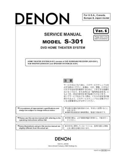
                                                                             For U.S.A., Canada,
                                                                             Europe & Japan model


                                                                                      Ver. 6
                               SERVICE MANUAL                                        Please refer to the


                                                        S-301
                                                                                     MODIFICATION NOTICE.

                             MODEL
                          DVD HOME THEATER SYSTEM


          HOME THEATER SYSTEM (S-301) consists of DVD SURROUND RECEIVER (ADV-S301),
          SUB WOOFER (DSW-S301) and SPEAKER SYSTEM (SC-S301)


For purposes of improvement, specifications and
design are subject to change without notice.


Please use this service manual with referring to the
operating instructions without fail.


Some illustrations using in this service manual are
slightly different from the actual set.


                                               TOKYO, JAPAN
                                    Denon Brand Company, D&M Holdings Inc.

                                                                                    X0245 V.06 DE/CDM 0612
                                                                                                                                            S-301


  SAFETY PRECAUTIONS
  The following check should be performed for the continued protection of the customer and service technician.

  LEAKAGE CURRENT CHECK
  Before returning the unit to the customer, make sure you make either (1) a leakage current check or (2) a line to chassis
  resistance check. If the leakage current exceeds 0.5 milliamps, or if the resistance from chassis to either side of the power
  cord is less than 460 kohms, the unit is defective.

  LASER RADIATION
  Do not stare into beam or view directly with optical instruments, class 3A laser product.


 CAUTION           Please heed the points listed below during servicing and inspection.

   Heed the cautions!                                                   Inspect for safety after servicing!
Spots requiring particular attention when servicing, such as         Check that all screws, parts and wires removed or discon-
the cabinet, parts, chassis, etc., have cautions indicated on        nected for servicing have been put back in their original posi-
labels or seals. Be sure to heed these cautions and the cau-         tions, inspect that no parts around the area that has been
tions indicated in the handling instructions.                        serviced have been negatively affected, conduct an insulation
                                                                     check on the external metal connectors and between the
   Caution concerning electric shock!                                blades of the power plug, and otherwise check that safety is
                                                                     ensured.
(1) An AC voltage is impressed on this set, so touching inter-
    nal metal parts when the set is energized could cause
                                                                     (Insulation check procedure)
    electric shock. Take care to avoid electric shock, by for ex-
                                                                     Unplug the power cord from the power outlet, disconnect the
    ample using an isolating transformer and gloves when
                                                                     antenna, plugs, etc., and turn the power switch on. Using a
    servicing while the set is energized, unplugging the power
                                                                     500V insulation resistance tester, check that the insulation re-
    cord when replacing parts, etc.
                                                                     sistance between the terminals of the power plug and the ex-
(2)There are high voltage parts inside. Handle with extra care       ternally exposed metal parts (antenna terminal, headphones
    when the set is energized.                                       terminal, microphone terminal, input terminal, etc.) is 1M or
                                                                     greater. If it is less, the set must be inspected and repaired.
   Caution concerning disassembly and assembly!
Though great care is taken when manufacturing parts from
sheet metal, there may in some rare cases be burrs on the
edges of parts which could cause injury if fingers are moved          CAUTION          Concerning important safety parts
across them. Use gloves to protect your hands.
                                                                     Many of the electric and structural parts used in the set have
   Only use designated parts!                                        special safety properties. In most cases these properties are
                                                                     difficult to distinguish by sight, and using replacement parts
The set's parts have specific safety properties (fire resis-         with higher ratings (rated power and withstand voltage) does
tance, voltage resistance, etc.). For replacement parts, be          not necessarily guarantee that safety performance will be pre-
sure to use parts which have the same properties. In particu-        served. Parts with safety properties are indicated as shown
lar, for the important safety parts that are marked ! on wiring      below on the wiring diagrams and parts lists is this service
diagrams and parts lists, be sure to use the designated parts.       manual. Be sure to replace them with parts with the designat-
                                                                     ed part number.
   Be sure to mount parts and arrange the
   wires as they were originally!                                    (1) Schematic diagrams ... Indicated by the ! mark.
For safety reasons, some parts use tape, tubes or other insu-        (2) Parts lists ... Indicated by the ! mark.
lating materials, and some parts are mounted away from the
                                                                                      Using parts other than the designated parts
surface of printed circuit boards. Care is also taken with the
                                                                                      could result in electric shock, fires or other
positions of the wires inside and clamps are used to keep
                                                                                      dangerous situations.
wires away from heating and high voltage parts, so be sure to
set everything back as it was originally.


                                                                                                                                        2
                                                            S-301


DISASSEMBLY
(Follow the procedure below in reverse order when
reassembling.)

1. Loader Panel
 (1) Switch on, and press [     (OPEN/CLOSE)] button
     to open the Disc tray.
 (2) Detach the Loader Panel by lifting.


2. Side Panel, Bottom Cover
 (1) Remove 13 bottom screws.
 (2) Remove 7 rear screws, then detach Side Panel and
     Bottom Cover.


                                                        3
                                                            S-301

3. Top Cover
(1) Remove 9 top screws, then detach Top Cover.


4. Front Panel Ass'y
(1) Remove 3 Front panel screws, then detach P.W.B.
    and chassis.
(2) Remove 4 Front panel side screws, then detach the
    Front Panel Ass'y.


5. Front Panel Ass'y
(1) Remove each terminal screws, Back Panel screws
    and Chassis screws, then detach the Back Panel.


                                                        4
                                                                                       S-301

6. DVD Mecha
(1) Remove 4 screws, then detach P.W.B.(1U-3695-1,
    1U-3695-2, 1U-3695-3) and TUNER PACK.


                                                             1U-3695-3

                                 TUNER PACK


                                                                           1U-3695-1


                                                                          1U-3695-2


(2) Remove 6 screws, then detach 1uU-3692 P.W.B.
    with DVD mecha from bottom chassis.


                                                         DVD mecha


                                                                1U-3692


                                                     5
                                                             S-301

7. Traverse Unit Disassembly
     Caution: The optical pickup can be damaged easily
     by static electricity charged on human body. Take
     necessary anti-static measures when repairing
     around the optical pickup.

7.1. Guide Clamp Bracket disassembly
(1) Remove 2 screws.
(2) Remove Guide Clamp Bracket to arrow direction.


7.2. Tray disassembly
(1) Remove to arrow direction.
(2) Solder the short-circuit (see in the frame).


                                                         6
                                                                              S-301

7.3. Traverse Unit disassembly
(1) Remove 24P FFC (CX241), 15P FFC (CX151), 5P
    PH WIRE (CX051) connecting with from 1U-3692
    P.W.B.
(2) Remove 4 screws fixing Damper.
(3) Remove Traverse Unit to arrow direction.


                                                             1U-3692 P.W.B.


Note for disassembly Traverse Unit
(1) When assembling, reverse the order of the above.
(2) When inserting Tray, confirm boss on Slide Cam
    set to ditch of the Tray (Compare with below draw-
    ing).


                                                         7
                                                                         S-301


DIAGNOSTICS OF OPTICAL PICKUP
AND REPLACING TRAVERSE UNIT
 Make failure diagnostics of the Optical Pickup as follows.
 If the laser drive current (Iop) becomes more than 1.5 times of
 the initial value, the Optical Pickup should be replaced.
 The laser drive current is registered on the seal attached to the
 rear of the Mecha.Unit.
 In case of replacing the Pickup, change the whole part of the
 Traverse Unit.
 No mechanical adjustment is necessary after the replace-
 ment.


                                   Example:         DVD 30mA
                                                    CD 30mA


      Disc no read, unsteady playback, etc.


     Laser drive current (Iop) check
     HF wave form check
     (Refer to WAVE FORMS)


                       Present value exceeds the ini-
                       tial value by 1.5 times


     Traverse Unit replacing
     (See page 6, 7 for details)


     Laser current registering after replacement.


    Step: Disc playback
    Write the measured value on the seal attached to the
    Mecha. Unit
    * As to the measuring method, refer to page 9, 10.


                                                                     8
                                                                                                             S-301

1. Label Indication of SACD Mechanism.


                                                                      Laser current consumption value

                                                                      ex) DVD         mA, CD            mA


                                                                          DVD         mA, CD            mA


2. Note for Handling the Laser Pick-Up
  The protection for the damage of laser diode.
  If you want to change the optical device unit from any other
  units, you must keep the following.
 (1) It should be done at the desk already took measures the
      static electricity in care of removing the OPU's (Optical
      device unit) connector cable.
 (2) Workers should be put on the "Earth Band".
 (3) It should be done to add the solder to the short land to
      prevent the broken Laser diode before removing the 24P
      FFC cable.
 (4) Don't touch OPU's connector parts carelessly.


3. Replacement of the Laser Pick-up
   (Traverse Unit)
 Check the Iop (Laser drive current)
 If the present Iop (current) value exceeds.+150% of the ini-
 tial value, replace the Traverse unit (Laser Pick-up) with a
 new one.


4. Iop Measurement Method
 When measuring Laser drive current (Iop), playback the
 discs (CD,DVD) described below, measure Iop for CD Laser
 and DVD Laser by the test point (+5V-A2~ LD (CD), LD
 (DVD))on the Main P.W.B.


 Test Disc : DVD/DVDT-S01 or commercially available
             discs.
           : CD/TCD-784 (manufactured by ALMEDIO
             INC) or commercially available discs.


                                                                  9
                                                                                                                                  S-301

4.1. DVD Laser current measurement


LD (DVD)                                                                                                LD (DVD)
 +5V-A2                                                                                                   +5V-A2
                                                            Oscilloscope                                           Oscilloscope

(1) Connect the oscilloscope to +5V-A2 of test point for
    GND side and LD (DVD) of test point for signal side.
(2) Playback the multi layer track 1 of the DVD Test Disc.
(3) Measure the voltage between +5V-A2 and LD (DVD),
    calculate Iop by the formula as shown below.


           Measurement Voltage Value
     Iop = ----------------------------------------------------------------------------
                                                                                      -
                    14 (Resistance value)


4.2. CD Laser current measurement
(1) Connect the oscilloscope to +5V-A2 of test point for
    GND side and LD (CD) of test point for signal side.
(2) Playback the track 1 of the CD Test Disc.
(3) Measure the voltage between +5V-A2 and LD (CD), cal-
    culate Iop by the formula as shown below.


           Measurement Voltage Value
     Iop = ----------------------------------------------------------------------------
                                                                                      -
                11.75 (Resistance value)


                                                                                                                             +5V_A2


                                                                                                                             LD(CD)


                                                                                                                             LD(DVD)


                                                                                          1u-3692 foil side

                                                                                                 10
                                                                  S-301


Special operating procedures
1. Initialization
    This initializes the data for the function, volume,
    DVD mechanism (RL-874), etc.
 (1) Check that the AC cord is disconnected from the
     power outlet. (AC OFF)
 (2) While pressing the FUNCTION and OPEN/CLOSE
     ( ) buttons on the main unit, plug the AC cord into
     the power outlet. (AC ON)
 (3) Check that the entire display and all the LEDs light,
     then release the FUNCTION and OPEN/CLOSE
     ( ) buttons.
 (4) After about 3 seconds, "INITIALIZE" appears on the
     display.
 (5) After initialization is complete (when "INITIALIZE"
     turns off), the function is set to "DVD" and the vol-
     ume level is set to       ("-dB" is displayed).


2. System check mode
    Use this to display the version information, etc.
 (1) In the standby mode, while pressing the STOP ( )
     and A.FWD (        ) buttons on the main unit, press
     the ON/STANDBY button.
 (2) Press the STATUS button on the remote control
     unit (RC-1005 or RC-1006) to display the following
     information, in this order: Time (TIME)     System
     microprocessor version (SYS Ver)        Date of sys-
     tem microprocessor version updating (SYS Date)
        DSP version (DSP Ver)       Date of DSP version
     updating (DSP Date)       Date of drive microproces-
     sor version updating (Dr Date) ESS version (Ess
     Ver) Date of ESS version updating (Ess Date)
     Region number (Region No.)
 (3) To cancel, unplug the AC cord. (AC OFF)
     NOTE 1: The DVD mechanism driver version and
             ESS version are not displayed unless the
             function is once set to DVD.


                                                             11
                                                                    S-301


ADJUSTMENT
1. SETTING
 (1) Connect the oscilloscope to the Y-signal, PB-signal and
     CB-signal, PR-signal and CR-signal of ZONE2 COMPO-
     NENT OUT terminal and each terminate at 75 Ohms.
        Use the 75 Ohms resistance must be 1%
 (2) DVD test disc : DVDT-S01
 (3) S OUT of DVD player is connected to AUX1 S IN.


2. Before Adjustment
 2.1. Setting the Oscilloscope as below.
 (1) PB/CB, PR/CR
   (a) TIME/DIV     :   10 s
   (b) VOLT/DIV : 100mV
       (Use the probe : x10 )
 (2) Y
   (a) TIME/DIV     :   10 s
   (b) VOLT/DIV : 200mV
       (Use the probe : x10 )
   Power on. Power Supply
   USA & Canada :          120V
   Europe           :      230V
   Japan            :      100V
   China & Korea :         220V

 2.2. Setup the DVD player and confirmation of the
      stators
 (1) Set to "INTERLACED" mode at the COMPONENT OUT.
 (2) Confirm the DVD player's out put level is equal as the
     item 2.4. in following.


 2.3. Preparation
 (1) Push the FUNCTION knob to select "AUX1" input.
 (2) Push [OPEN/CLOSE] button of DVD player, then open
     the Disc Tray.
     Set DVD test disc (DVDT-S01) on the Disc Tray, and
     then push [CLOSE] button.
 (3) DVD player FL display appear "STOP", push [PLAY] but-
     ton to playback DVD.
 (4) Push the [DISPLAY] button of remote control of DVD
     player unit and then appear the ON-Screen Display (GUI)
     on the monitor TV.
 (5) Push the [+10] and [2] button, select Title 12 of DVD.
 (6) Push the [ENTER] button, playback Title 12.
     (color bar 75%)


                                                               12
                                                             S-301

2.4. Procedure
(1) Adjust the signal of COMPONENT OUT by the wave of
    oscilloscope.
 (a) Target, Y-signal
     Point               :    1U-3695-3 VR601
     Adjustment Value    :    714   35mV
     Waveform


                                 Y


             Y-signal COMPONENT OUT


 (b) Target, PB/CB-signal
     Point              :     1U-3695-3 VR602
     Adjustment Value :       *525   25mV
     Waveform


                                 PB


           PB/CB-signal COMPONENT OUT


 (c) Target, PR/CR-signal
     Point              :     1U-3695-3 VR603
     Adjustment Value :       *525   25mV
     Waveform


                                     PR/CR


      PR/CR-signal COMPONENT OUT

 * : 486     10mV for U.S.A. & Canada model


                                                        13
                                          S-301


BLOCK DIAGRAM


                IN
                DATP20:FL/FR
                DAIP19:C/SW
                DAIP18:SL/SR


                  OUT
                  DAIP16:FL/FR
                  DAIP16:0/SW
                  DAIP15:0/0
                  DAIP14:RECL/RECR


                                     14
                     S-301


LEVEL DIAGRAM


                15
                                                                                                                                   1. IC's


                                         LCS0#


                                             LA3
                                             LA2
                                             LA1
                                             LA0
                                       LWRLL#
                                            LD11
                                           LOE#


                                         LCS3#
                                         LCS2#
                                         LCS1#


                                             VSS
                                             VEE
                                             VSS
                                             VEE
                                             VSS
                                             VSS
                                             VEE
                                             VSS
                                             VSS
                                             VEE
                                             VSS
                                             VEE
                                             VEE


                                        CAMIN1
                                        CAMIN0
                                       LWRHL#
                                            LD15
                                            LD14
                                            LD13
                                            LD12
                                            LD10
                                             LD9
                                             LD8
                                             LD7
                                             LD6
                                             LD5
                                             LD4
                                             LD3
                                             LD2
                                             LD1
                                             LD0
                                    AUX[3]/IOR#
                                    AUX[2]/IOW#
                                 I2CDATA/AUX[0]


                                            VCC
                                     HA2/AUX4[4]


                                         AUX[7]
                                         AUX[6]
                                         AUX[5]
                                         AUX[4]
                                 I2C_CLK/AUX[1]


                                 208
                                 207
                                 206
                                 205
                                 204
                                 203
                                 202
                                 201
                                 200
                                 199
                                 198
                                 197
                                 196
                                 195
                                 194
                                 193
                                 192
                                 191
                                 190
                                 189
                                 188
                                 187
                                 186
                                 185
                                 184
                                 183
                                 182
                                 181
                                 180
                                 179
                                 178
                                 177
                                 176
                                 175
                                 174
                                 173
                                 172
                                 171
                                 170
                                 169
                                 168
                                 167
                                 166
                                 165
                                 164
                                 163
                                 162
                                 161
                                 160
                                 159
                                 158
                                 157
                     VEE     1                    156   VSS
                      LA4    2

                                                                                       PINOUT DIAGRAM
                                                  155   HA1/AUX4[3]
                      LA5    3                    154   HA0/AUX4[2]
                      LA6    4                    153   HCS3FX#/AUX3[6]
                      LA7    5                    152   HCS1FX#/AUX3[7]
                      LA8    6                    151   HIOCS16#/CAMCLK/AUX3[4]
                                                                                                        ES6138F (IC101: 1U-3692)


                      LA9    7                    150   HRD#/DCI_ACK#/AUX4[6]
                     VSS
                                                                                                                                                                                                                                     SEMICONDUCTORS /


                             8                    149   HWR#/DCI_CLK/AUX4[5]
                     VCC     9                    148   VEE
                    LA10    10                    147   VSS
                     LA11   11                    146   HIORDY/AUX3[3]
                    LA12    12                    145   HRST#/AUX3[5]
                    LA13    13                    144   HIRQ/DCI_ERR#/AUX4[7]
                    LA14    14                    143   HRRQ#/AUX4[0]
                    LA15    15                    142   HWRQ#/DCI_REQ#/AUX4[1]
                    LA16    16                    141   HD15/AUX2[7]/IR
                     VSS    17                    140   HD14/AUX2[6]
                     VEE    18                    139   VCC
                    LA17    19                    138   VSS
                    LA18    20                    137   HD13/AUX2[5]/SP
                    LA19    21                    136   HD12/AUX2[4]/C2PO
                    LA20    22                    135   HD11/AUX2[3]//IRQ
                    LA21    23                    134   HD10/AUX2[2]
                 RESET#     24                    133   HD9/AUX2[1]
            TDMDX/RSEL      25                    132   HD8/DCI_FDS#/AUX2[0]/VFD_CLK
                     VSS    26                    131   HD7/DCI7/AUX1[7]/VFD_DIN


16
                     VEE    27                    130   VEE
                  TDMDR     28                    129   VSS
                 TDMCLK     29                    128   HD6/DCI6/AUX1[6]/VFD_DOUT
                  TDMFS     30                    127   HD5/DCI5/AUX1[5]
               TDMTSC#      31                    126   HD4/DCI4/AUX1[4]


                                        ES6138F
           TWS/SEL_PLL2     32                    125   HD3/DCI3/AUX1[3]
          TSD0/SEL_PLL0     33                          HD2/DCI2/AUX1[2]
                                                  124
                     VSS    34                          HD1/DCI1/AUX1[1]
                                                  123
                     VCC    35                          HD0/DCI0/AUX1[0]
                                                  122
          TSD1/SEL_PLL1     36                          VCC
                                                  121
                    TSD2    37                          VSS
                                                  120
                    TSD3    38                          HSYNC#/CAMIN7/AUX3[0]
                                                  119
                   MCLK     39                          VSYNC#/CAMIN6/AUX3[1]
                                                  118
                   TBCK     40                          PCLKQSCN/CAMIN5/AUX3[2]
                                                  117
                                                                                                                                             Only major semiconductors are shown, general semiconductors etc. are omitted to list.


     SEL_PLL3/SPDIF_OUT     41                          PCLK2XSCN/CAMIN4
                                                  116
                SPDIF_IN    42                          YUV7/FDAC/CAMIN3
                                                  115
                     VSS    43                          YUV6/VDAC
                                                  114
                     VCC    44                          YUV5/YDAC
                                                  113
                     RSD    45                          ADVSS
                                                  112
                    RWS     46                          ADVEE
                                                  111
                   RBCK     47                          YUV4/RSET
                       NC                         110
                            48                    109   YUV3/COMP
                      XIN   49                    108   YUV2/CDAC
                   XOUT     50                    107   YUV1/VREF
                    AVEE    51                    106   YUV0/CAMIN2/UDAC
                    AVSS    52                    105   DCLK


                                  55
                                  56
                                  58
                                  59
                                  60
                                  61
                                  62
                                  65
                                  68


                                  57


                                  53
                                  54
                                  91
                                  93
                                  94
                                  96


                                  63
                                  64
                                  66
                                  67
                                  69
                                  70
                                  71
                                  72
                                  73
                                  74
                                  75
                                  76
                                  77
                                  78
                                  79
                                  80
                                  81
                                  82
                                  83
                                  84
                                  85
                                  86
                                  87
                                  88
                                  89
                                  90
                                  92
                                  95
                                  97
                                  98
                                  99
                                 100
                                 101
                                 102
                                 103
                                 104


                                 DB0
                                 DB1
                                 DB2
                                 DB3
                                 DB4
                                 DB5
                                 DB6
                                 DB7
                                 DB8
                                 DB9


                                 VEE
                                 VSS
                                 VSS
                                 VEE
                                 VEE
                                 VSS
                                 VSS
                                 VSS
                                 VEE
                                 VSS
                                 VEE
                                 VSS
                                 VEE


                                 VCC
                                 DQM


                                 DB11
                                 DB10
                                 DB12
                                 DB13
                                 DB14
                                 DB15
                                 DSCK


                                 DMA0
                                 DMA1
                                 DMA2
                                 DMA3
                                 DMA4
                                 DMA5
                                 DMA6
                                 DMA7
                                 DMA8
                                 DMA9
                                 DWE#
                                 DCS1#
                                 DCS0#


                                 DMA11
                                 DMA10
                                 DCAS#
                                 DRAS#
                                 DMBS1
                                 DMBS0

                                 DOE#/DSCK_EN
                                                                                                                                                                                                                                                        S-301
                                                                                                                     S-301


ES6138F Pin Description
Name              Pin Numbers          I/O   Definition
VEE            1,18, 27, 59, 68, 75,
                92, 99, 104, 130,
                                       P     I/O power supply.
               148, 157, 159, 164,
                  183, 193, 201
                2:7, 10:16, 19:23,
LA[21:0]                               O     RISC port address bus.
                     204:207
VSS             8, 17, 26, 34, 43,
                60, 67, 76, 84, 91,
                98, 103, 120, 129,
                                       G     Ground.
               138, 147, 156, 163,
               171, 177, 184, 192,
                     200, 208
                9, 35, 44, 83, 121,
VCC                                    P     Core power supply.
                     139, 172
RESET#                  24              I    Reset input (active-low).
TDMDX                                  O     TDM transmit data output.
RSEL                                    I    LCS3 ROM Boot Data Width Select. Strapped to VCC or ground via 4.7-k
                                             resistor; read only during reset.
                        25                             RSEL            Selection

                                                           0         16-bit ROM
                                                           1         8-bit ROM


TDMDR                   28              I    TDM receive data input.
TDMCLK                  29              I    TDM clock input.
TDMFS                   30              I    TDM frame sync input.
TDMTSC#                 31             O     TDM output enable (active-low).
TWS                                    O     Audio transmit frame sync output.
SEL_PLL2                                I    System and DSCK output clock frequency selection is made at the rising edge of
                                             RESET#. The matrix below lists the available clock frequencies and their
                                             respective PLL bit settings. Strapped to VCC or ground via 4.7-k resistor; read
                                             only during reset.

                                                 SEL_PLL2           SEL_PLL1     SEL_PLL0     PLL Settings
                                                       0               0            0          DCLK 


◦ Jabse Service Manual Search 2026 ◦ Jabse PravopisonTap.bg ◦ Other service manual resources online : FixyaeServiceinfo