Service Manuals, User Guides, Schematic Diagrams or docs for : Embest STDV710A
<< Back | HomeMost service manuals and schematics are PDF files, so You will need Adobre Acrobat Reader to view : Acrobat Download Some of the files are DjVu format. Readers and resources available here : DjVu Resources
For the compressed files, most common are zip and rar. Please, extract files with Your favorite compression software ( WinZip, WinRAR ... ) before viewing. If a document has multiple parts, You should download all, before extracting.
Good luck. Repair on Your own risk. Make sure You know what You are doing.
Image preview - the first page of the document
>> Download STDV710A documenatation <<
Text preview - extract from the document
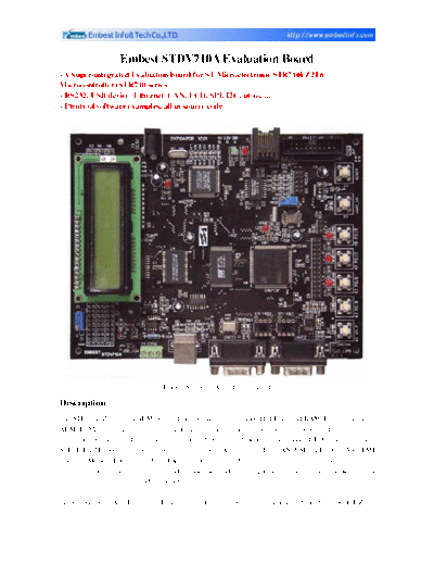
                     Embest STDV710A Evaluation Board
- A Super-integrated Evaluation board for ST Microelectronic STR710FZ2T6
Microcontroller (STR710 series)
- RS232, USB device, Ethernet, CAN, LCD, SPI, I2C, uCos, ...
- Plenty of software examples, all in source code


                                     Embest STDV710A Evaluation Board

Description
The STR710F-Z2T6 is an ARM-powered microcontroller with embedded Flash and RAM. It is based on the
ARM7TDMI core with low pin-count packages to aim at customers who want the power and flexibility of a
32-bit microcontroller plus an extensive range of peripheral functions and enhanced I/O capabilities. The
STR710F-Z2T6 with high connectivity is using various interfaces including CAN, USB, SPI, I2C, UART, EMI
(External Memory Interface) and etc. The controller is designed to target industrial control applications such as
factory automation, point-of-sale and vending machines, and testing equipment, as well as mass-market telecom
applications such as bridges and protocol translators.

Embest STDV710ATM Evaluation Board is intended as a low cost evaluation platform for STR710F-Z2T6


                                                                                                               1
devices. The board expands all features of STR710F-Z2T6 microcontroller and support various additional
peripherals including 512k Bytes SRAM and 2M bytes flash on EMI. It integrates LEDs, buzzer, test buttons,
LCD, Ethernet, CAN, SPI, I2C, USB interfaces to create a versatile stand-alone test platform. Users can fully
take use of the board to meet your development requirements and applications. The Embest STDV710A
Evaluation Board Kit is a complete development environment contains an evaluation board, a JTAG debugger
interface and a plenty of sample programs for embedded development.


Hardware Specification
        Dimensions: 163x124mm
        Working temperature: -40~+85 Celsius
        Processor: STR710F-Z2T6 with embedded 272kByte (256k+16k) FLASH memory and 64kByte SRAM
        memory
        Power input: +5.0V/1A
        16-bit EMI SRAM: 256k 16-bit EMI Nor Flash: 1M
        10M Ethernet interface (CS8900)
        USB2.0 full speed (12Mbs) interface
        CAN2.0 communication interface with CAN driver-chip
        UART0 and UART2 with 2 RS232 ports (can interconnect to each other for RS232 communication
        experiment)
        Serial Peripheral Interface- SPI (flash chip is able to plug in and out for replacement)
        II-C interface (EEPROM chip is able to plug in and out for replacement) and HDLC interface reuse
        16x2 Character LCD or 128x64 Dot-matrix LCD
        5 LED indicator light: one for power, one for standby, three others are general used
        4 channel ADC and 1 on-board regulator (ADC experiment)
        1 buzzer (PWM experiment)
        1 Reset button
        1 WAKE-UP button
        5 general used keys
        32 CPU multi-functional reused I/O expansion (HDLC, Smart Card, etc.)
        IAP (In Application Programming) function
        A standard 20-pin Debug-JTAG connector


Interfaces and Jumpers Introduction


                                                                                                           2
Interfaces: List below the introduction of the main interfaces
                 Interface        Name                    Description
                     J1           LCD                    LCD interface
                     J2        BUF_BUS         8-bit data bus interface with buffer
                     J3          DC5V                    Power DC5V
                     J4           CAN            CAN communication interface
                     J5           USB               USB (Device) interface
                     J6          UART0                    Serial port 0
                     J7           RJ45              10M Ethernet interface
                     J8          UART2                    Serial port 2
                     J9           JTAG                   JTAG interface
                    J10         ADC/P1                   ADC interface
                    J11           GPIO                 General I/O ports


Jumpers: List below the functions and settings of the main interfaces
   Jumper    Description      Setting                       Setting explanation


                                                                                      3
                  USB                             Power supplied by USB interface without external power
     JP1                          Short-circuit
                EXT-Power                         supply
                                  Disconnection   Power supplied by external power connection
                                  Short-circuit   Connected to enable buzzer to work
     JP2      Buzzer Enable
                                  Disconnection   Disable buzzer
                 CAN              Short-circuit   Enable 120CAN matched resistance
     JP3       MATCHED
                                  Disconnection   Disable CAN matched resistance
              RESISTANCE
     JP4        BOOT EN
     JP5            BOOT0                           Reference to BOOT MODE SETTING
     JP6            BOOT1
              Reset Signal to
     JP7                                               Reference to /TRST and /RESET
               Short-circuit
     JP8        IAP Enable                                 Reference to IAP Enable


BOOT MODE SETTING

   BOOT      BOOT1      BOOT0                       Boot memory
                                      Mode                                            Explanation
    EN        (B1)       (B0)                         mapping
     0         any          any                     On-chip Flash
                                       user                             System boot from on-chip flash
     1          0           0                      mapping to add0
                                                                        System boot from pre-loaded booting
                                    System         System memory
     1          0           1                                           program;
                                    memory         mapping to add0
                                                                        Clock being frozen
                                                  On-chip SRAM          System boot from on-chip SRAM;
     1          1           0         RAM
                                                  mapping to add0       Used in lab development
                                    External      External memory       System boot from external memory
     1          1           1
                                    memory        mapping to add0       (viz. external Flash of the board)


/TRST and /RESET
/TRST is the reset signal for the controller when debugging use the JTAG interface. /RESET is the reset signal
for CPU peripherals including on-chip and external. JP7 on board is used for the two reset signals. Considering
stability while debugging, JP7 is short-circuited on the back of the board and is of no use. If users don't want to
reset peripherals, you can chop up conjunctive wire on the back of the board. But you should note that JP7 be
short-circuited when running offline to assure reset controller while power-up reset.

IAP Enable


P1.8 of GPIO is used for enabling IAP program. If on-chip Flash is burned with IAP program which is provided
with the board, to short-circuit JP8 to active IAP function when resetting. (Boot mode should set from on-chip


                                                                                                                 4
flash booting.)
Note: The definition of this jumper is only valid when running IAP program. User program can use this
jumper for other purposes.


STR710F Series Microcontroller Function Block Diagram


STR710F Series Device Summary


                                                                                                    5
Software Examples
Embest Provides plenty of software examples for this STDV710A evaluation board, all in source code. Each
program has two versions to correspond respectively with ADS and Embest environments. Separately saved
under the "ADS" and "Embest" sub-directories. The structure of the directories is as below:
                   Directory                                 Content
            ADS                       All source codes under ADS environment
            |--ADC                    ADC test program
            |--CAN                    CAN test program
            | |--CAN_LOOP             Loop-back mode test program
            | |__CAN_TX               Communicate with another device test program
                                      Common file including driver modules of main
            |--COMMON
                                      peripheral equipments
            | |--LwIP                 Source code porting by LwIP from STR71x
            | |--str71x               Driver modules of STR71x on-chip peripherals
            | |--uCOS_II              Source code porting by
◦ Jabse Service Manual Search 2024 ◦ Jabse Pravopis ◦ onTap.bg ◦ Other service manual resources online : Fixya ◦ eServiceinfo