Service Manuals, User Guides, Schematic Diagrams or docs for : HP V2000 POWER ON SEQUENCE STEP WISE FINAL NOTES
<< Back | HomeMost service manuals and schematics are PDF files, so You will need Adobre Acrobat Reader to view : Acrobat Download Some of the files are DjVu format. Readers and resources available here : DjVu Resources
For the compressed files, most common are zip and rar. Please, extract files with Your favorite compression software ( WinZip, WinRAR ... ) before viewing. If a document has multiple parts, You should download all, before extracting.
Good luck. Repair on Your own risk. Make sure You know what You are doing.
Image preview - the first page of the document
>> Download V2000 POWER ON SEQUENCE STEP WISE FINAL NOTES documenatation <<
Text preview - extract from the document
INTERSOFT LAPTOP CHIP LEVEL TRAINING +91 9824144698, 91 261 2424396
HP laptop v2000 dv1000 notebook power detail Step with timing
INTERSOFT INSTITUTE
LEARN CHIP LEVEL TRAINING (OFFLINE/ONLINE)
THE FIRST IN LAPTOP SERVICE TRAINING IN INDIA
INTERSOFT INSTITUTE
4, ANUPAMCHAMBERS, OPP. WOW COLLECTION, BHAGATALAO MAIN
ROAD, SURAT-395003 GUJARAT, INDIA
PHONE :- +91 261 2424396 MOBILE :- +91 9824144698/9824044699
WEB SITE :- http://intersoftelectronics.com
E.MAIL :- [email protected], [email protected]
Mobile, Computer, Data recovery, Printer Training Also Available
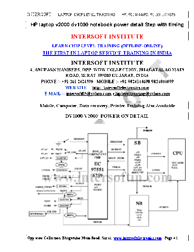
DV1000/V2000/ POWER ON DETAIL
Opp wow Collection, Bhagatalao Main Road, Surat. www.intersoftelectronics.com Page # 1
Opp wow Collection, Bhagatalao Main Road, Surat. www.intersoftelectronics.com Page # 2
1 PD21 VIN18V
+91 9824144698, 91 261 2424396
AC Charge PQ44 Battery
V 2000/ DV1000/ M2000 MOTHERBOARD TRACING DETAIL
1
158
Y8 160
Pin2 I/O SUS ON
2 NBSWON# PC87591L MAX1772
5 SUS ON HWPG EET
POWERCHIP HWPG
VREF 3V/5V
28
7 6
BATTERYCHIP
Pin4
PRIMARY VOLTAGE
Power Button
DNBSWON#
3 4
MAX1999/8734 3V PCU
SUSB
VIN
SUSC
ALWAYS
2 Pgood ON
6 SHDN VIN 3V SUSP
18, 5 VAL MAIN 3VSUS(AL4)
5VAL 3, 4 on 5V PCU
Pin6
LAPTOP CHIP LEVEL TRAINING
VIN +5V SUSP
MAIN 5VSUS
South Bridge SECONDRY VOLTAGE
2.5V SUS
MAX1845
ON2 Pin11
AB6 AC6 AC6
ON1 VIN
Pin12
7 HWPG 1.5V
Y6 Pin7
P RON
W
AC6
CPU PWRGD
32.768KHZ MAIN +1.5V
VRM
VIN
PWRON
VRON
SHDN
D6 Pin7
7 PCI RESET MAX1907 CPU CORE
North Bridge VRM VCC
8 CORE
1.36V
INTERSOFT
25 AMP
CPU VIO
INTERSOFT LAPTOP CHIP LEVEL TRAINING +91 9824144698, 91 261 2424396
First Step is to check whether normal voltage VA is generated. (VA is the voltage through PJ1 Power
Connector Adapter for Input Voltage.)If the Diode PD21, PD22 is open then VA voltage will not be
generated in normal circumstance.
Second Step is to check whether the VIN voltage is normal. VIN voltage is the voltage from the VA
conduction through the controlling MOSFET PQ44.
Third Step is to check 3.3/5 VPCU voltage is normal at Max 1999/8734. VIN voltage is generated as
3.3/5 VPCU in the basic premise of the system voltage. However, it only produces the two basic
voltages necessary for the condition to up the power section.
Here, we take the MAX8734/1999 chip as an example :
1. Check whether the MAX 1999/8734 20 PIN has 19V input.
2. Check whether the chip's first 6 PIN SHDN has high 5V. When the pin is low, the MAX8734
/1999 will shut down and stop working.
3. Check whether the chip 5V-AL PIN 18 of MAX 1999/8734 generates a linear voltage. Here we
have to note that the section of 5V-AL voltages should not be taken to mean 5VPCU voltage. As
a linear voltage, it's current output is very small, which is available in the 3.3/5 VPCU voltage
generator's start voltage before it. When the 3.3/ 5VPCU voltage stabilizes, the 5V-AL output
PIN voltage will be 5VPCU and will take over to provide power. If the PIN has normal voltage
output, then we can say that the MAX 1999/8734 internal line is up and working. If not, with the
exclusion of other chip pin under exceptional circumstances, consider replacing the MAX
1999/8734 power chip.
4. Now, check chip section On PIN 3,4 the ON3 and ON5 signal should be high.
The role of these two pins is to open the 3.3 VPCU and 5 VPCU voltages. If these 2 pins show
low here then they certainly would not have 3.3/ 5 VPCU voltage.
5. Check 3.3/5VPCU output voltage, short circuit to ground to check impedance of
the existence of such anomalies. If the voltage output is short circuit,
MAX1999/8734 will soon be in line to protect their own state, to stop the output
voltage.
6. Voltages examined on both sides of the MOS 3.3/5VPCU tube and connected to
control circuit is abnormal. We can examine and control ON3 and ON5 pins.
Opp wow Collection, Bhagatalao Main Road, Surat. www.intersoftelectronics.com Page # 3
INTERSOFT LAPTOP CHIP LEVEL TRAINING +91 9824144698, 91 261 2424396
Fig. System power main 5v 3v generate max 1999 schematic diagram
Fourth Step Check the Power Management chip, IO 87591L the first 44 PIN, the ACIN input pin on
the motherboard. This voltage on this pin must be high. Also check the power supply of the adapter to
the motherboard.
Fifth Step Press the start button on the power board, measure whether the power management chip's
first 2 PINS (ON/OFF NBSWON) high to low transition is working normally.
Sixth Step Check the power management chip to detect whether the first 4PIN (DNBSWON to South
Bridge) instant boot button is pressed. A high to low negative pulse transition should be detected. If not,
then this is an indication of trouble in the power management chip.
South Bridge received DNBSWON low, it occurs SUSB #, SUSC # 2 high sent to 97551/87591, South
Bridge chip part of the line is always in working confition. Likewise, it is also connected to a 32.768kHz
Y5, its role is to South Bridge chip modules RTC and basic detection module reference clock.
Opp wow Collection, Bhagatalao Main Road, Surat. www.intersoftelectronics.com Page # 4
INTERSOFT LAPTOP CHIP LEVEL TRAINING +91 9824144698, 91 261 2424396
Southbridge chip power management chip receiving the boot action to issue a pulse signal, this chip will
be the first 26PIN the S USB #, the first 69PIN high of SUSC # set to an invalid state, the power
management chip, boot up action to provide necessary conditions.
parts.
Seventh Step Check to ensure that SUSB# and SUSC# pin is in the high state from south bridge
received, . If one foot is in the low state, then it will be unable to achieve power management chip boot
action.
97551/87591 received SUSB #, SUSC # after have had a SUSON, MAINON #, VRON. SUSON
signals into SUSD signal sent tube arises 3VSUS, 5VSUS, and SUSON sent to MAX1845 generate
2.5VSUS.
MAINON # generated by PU7 SMDDR-VTERM. At the same time and by PQ119 PQ125 into MAIND
send PQ143, PQ145, PQ148, PQ153 produce +3 V, +5 V, +2.5 V, +1.5 V voltage.
VRON gave PU9 (MAX1907), PU5 (1992E) generated VCC-CORE and VCCP voltage. PU6, PU4
signals generated HWPG to 97,551, then PU3, PU5 also various feedback signals to generate a HWPG
97551/87591.
At this point the M / B of the main voltage in each group have been OK back HWPG voltage feedback
signal with convergence, the equivalent of a HWPG "and" relationship, such as including any group for
the low feedback HWPG this POWER OK 97551/87591 occurs
Fig. :- 2nd stage power supply block diagram
Eighth Step Measure, with a multi meter, the SUSON (from I/O to MAX1845, on signals 2nd stage 2.5
1.5 volt ) power management chip149 PIN low signal, to see whether there is a high jump in the signal.
This situation can be divided into two types: One is no action, the other is a jump, but without high
maintenance of the signal. On focused inspection of input pin voltage, we can see that the signal
generated is abnormal. The second case shows the power management chip to respond to the boot action
and begin to work up. But unfortunately the control module voltage generates a problem, it cannot
Opp wow Collection, Bhagatalao Main Road, Surat. www.intersoftelectronics.com Page # 5
INTERSOFT LAPTOP CHIP LEVEL TRAINING +91 9824144698, 91 261 2424396
generate the corresponding voltage and the voltage OK signal back to the power management chip. In
this case, the 63PIN HWPG (Power Good from MAX1845, MAX1999), under normal circumstances,
should send a high signal to the power management chip.
When the power management chip to the PWRGD signal received after a certain delay period, to again
PWROK signal to the corresponding delay circuit. Delay circuits at different delay, the order issued by
the appropriate power supply OK signal. One, SB-PWROK signal to the South Bridge chipm NB-
PWROK signal to the North Bridge chip. CPU-PWROK signal to CPU. Next, the system chipset will
issue a reset signal, First issued by the South Bridge PCIRST # signal to the PCI bus and other related
equipment and the North Bridge chip. Meanwhile, the North Bridge chip in the receiver to the South
Bridge chip issued PCIRST # reset signal, we will send CPURST# signal to the CPU.
Ninth Step in the boot power, the ultimate PWROK signal, (which is sent to the North , South and
MAX 1907 vrm chip). Power Management IC's 28 PIN is the pin we are looking for. Generally, if the
pin signal maintains a high signal, it indicates the boot was successful. The mother board's power supply
module and voltage stability are maintained.
Tenth Step when the instruction to turn off opening of voltage, such as the OK is HWPG constant as
high as 97,551, after receiving HWPG produce PWROK signal sent to SB Southbridge, Southbridge SB
produced after the PCI RST # generated through U42 PCIRST # passed to North Bridge. North Bridge
before they produce the CPURST #. Signal description, ^ & b: v3 (0 G
MAIN FOULT LIST WITH PARTICULAR ICS
Main fault: MAX 1999/8743 3VPCU or 5VPCU bad output (usually board plug 19vin, there are
two voltage output)
1. VIN_1999 input 19V voltage problems.
2. Test 8 pin reference voltage is 2V. ,?! D0 W-]: E '?) D) C
3. Check whether PQ103 PQ101 or bad.
4. Measured with a Multimeter or 5VPCU 3VPCU ground impedance, small or short-circuit
impedance for RMA board, the general line of parts for the burn. (PU10, PQ101, PQ103,
PQ104, PQ102, PQ105, U23, etc.). '' ^ & D & ^ 2 D O # ~. `2 V
The IC is a voltage generated 2.5VSUS and 1.5V_S5 two groups, in 19VIN added after S5_ON,
SUSON under normal circumstances, the two signals, that can generate the two voltages. 3 `0 k:
b1 i-E; B8 A
Main fault: MAX 1845 2.5VSUS or 1.5V_S5 output bad (not voltage output and low).
1. VIN_1845 input 19V voltage problems.
2. Open bad. 2
3. S5_ON, SUSON poor or no signals sent 1845IC. . O & z (b8 J8 X
4. 2.5 VSUS and 1.5V_S5 two smaller voltage-to-ground impedance or short circuit, for the RMA
board, the general line of parts for the burn (PU5, PQ82, PQ99, PQ83, PQ106, PQ87, U16)
Signal description!
is the speed of the IC chip power management control, supply CPU CORE voltage, can automatically
correct the offset, ◦ Jabse Service Manual Search 2026 ◦ Jabse Pravopis ◦ onTap.bg ◦ Other service manual resources online : Fixya ◦ eServiceinfo