Service Manuals, User Guides, Schematic Diagrams or docs for : Keithley Appnotes MaxThroughputSwitch_AppNote
<< Back | HomeMost service manuals and schematics are PDF files, so You will need Adobre Acrobat Reader to view : Acrobat Download Some of the files are DjVu format. Readers and resources available here : DjVu Resources
For the compressed files, most common are zip and rar. Please, extract files with Your favorite compression software ( WinZip, WinRAR ... ) before viewing. If a document has multiple parts, You should download all, before extracting.
Good luck. Repair on Your own risk. Make sure You know what You are doing.
Image preview - the first page of the document
>> Download MaxThroughputSwitch_AppNote documenatation <<
Text preview - extract from the document
Number 3089
Application Note Designing a High Throughput Switch System for
Series Semiconductor Measurements with the Model 707B
or 708B Semiconductor Switch Matrix Mainframe
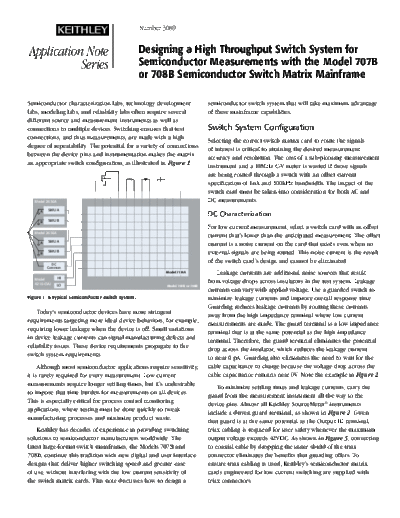
Semiconductor characterization labs, technology development semiconductor switch system that will take maximum advantage
labs, modeling labs, and reliability labs often require several of these mainframe capabilities.
different source and measurement instruments as well as
connections to multiple devices. Switching ensures that test Switch System Configuration
connections, and thus measurements, are made with a high
Selecting the correct switch matrix card to route the signals
degree of repeatability. The potential for a variety of connections
of interest is critical to attaining the desired measurement
between the device pins and instrumentation makes the matrix
accuracy and resolution. The cost of a sub-picoamp measurement
an appropriate switch configuration, as illustrated in Figure 1.
instrument and a 10MHz C-V meter is wasted if those signals
are being routed through a switch with an offset current
specification of 1nA and 100kHz bandwidth. The impact of the
switch card must be taken into consideration for both AC and
Model 2636A DC measurements.
SMU A
DC Characterization
A
B SMU B
For low current measurement, select a switch card with an offset
Model 2636A
current that's lower than the anticipated measurement. The offset
SMU A
A
current is a noise current on the card that exists even when no
B SMU B external signals are being routed. This noise current is the result
DC
of the switch card's design and cannot be eliminated.
Common
Model 7174A Leakage currents are additional noise sources that result
Model HI
4210-CVU from voltage drops across insulators in the test system. Leakage
LO Model 707B or 708B
currents can vary with applied voltage. Use a guarded switch to
Figure 1. A typical semiconductor switch system. minimize leakage currents and improve overall response time.
Guarding reduces leakage currents by routing these currents
Today's semiconductor devices have more stringent
away from the high impedance terminal where low current
requirements targeting more ideal device behaviors, for example,
measurements are made. The guard terminal is a low impedance
requiring lower leakage when the device is off. Small variations
terminal that is at the same potential as the high impedance
in device leakage currents can signal manufacturing defects and
terminal. Therefore, the guard terminal eliminates the potential
reliability issues. These device requirements propagate to the
drop across the insulator, which reduces the leakage current
switch system requirements.
to near 0 pA. Guarding also eliminates the need to wait for the
Although most semiconductor applications require sensitivity, cable capacitance to charge because the voltage drop across the
it is rarely required for every measurement. Low current cable capacitance remains near 0V. Note the example in Figure 2.
measurements require longer settling times, but it's undesirable
To minimize settling times and leakage currents, carry the
to impose that time burden for measurements on all devices.
guard from the measurement instrument all the way to the
This is especially critical for process control monitoring
device pins. Almost all Keithley SourceMeter◦ Jabse Service Manual Search 2026 ◦ Jabse Pravopis ◦ onTap.bg ◦ Other service manual resources online : Fixya ◦ eServiceinfo