Service Manuals, User Guides, Schematic Diagrams or docs for : Keithley Appnotes 2508 ChargePumping
<< Back | HomeMost service manuals and schematics are PDF files, so You will need Adobre Acrobat Reader to view : Acrobat Download Some of the files are DjVu format. Readers and resources available here : DjVu Resources
For the compressed files, most common are zip and rar. Please, extract files with Your favorite compression software ( WinZip, WinRAR ... ) before viewing. If a document has multiple parts, You should download all, before extracting.
Good luck. Repair on Your own risk. Make sure You know what You are doing.
Image preview - the first page of the document
>> Download 2508 ChargePumping documenatation <<
Text preview - extract from the document
A G R E AT E R M E A S U R E O F C O N F I D E N C E
A
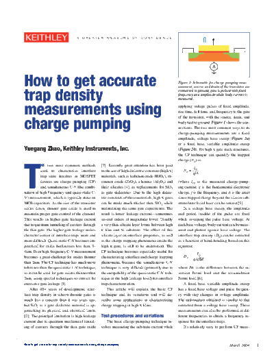
How to get accurate Figure 1: Schematic for charge pumping mea-
surement; source and drain of the transistor are
trap density
connected to ground; gate is pulsed with fixed
frequency and amplitude while body current is
measured.
measurements using applying voltage pulses of fixed amplitude,
rise time, fall time, and frequency to the gate
charge pumping
of the transistor, with the source, drain, and
body tied to ground. Figure 1 shows the con-
nections. The two most common ways to do
charge-pumping measurements are a fixed
amplitude, voltage base sweep (Figure 2a)
or a fixed base, variable amplitude sweep
Yuegang Zhao, Keithley Instruments, Inc. (Figure 2b). For high gate stack structures,
the CP technique can quantify the trapped
T
charge (Nit) as:
HE two most common methods [3]. Recently great attention has been paid
Icp
used to characterize interface to the use of high dielectric constant (high ) Nit = ___
qfA
trap state densities in MOSFET materials, such as hafnium oxide (HfO2), zir-
devices are charge pumping (CP) conium oxide (ZrO2), alumina (Al2O3) and (where Icp is the measured charge-pump-
and simultaneous C-V (the combi- their silicates [4], as replacements for SiO2 ing current, q is the fundamental electronic
nation of high frequency and quasi-static C- as gate dielectrics. Due to the high dielec- charge, f is the frequency, and A is the area)
V) measurement, which is typically done on tric constants of these materials, high gates since trapped charge beyond the silicon sub-
MOS capacitors. As the size of the transistor can be made much thicker than SiO2 while strate/interfacial layer can be sensed [5].
scales down, thinner gate oxide is used to maintaining the same gate capacitance. The In a voltage base sweep, the amplitude
maintain proper gate control of the channel. result is lower leakage current--sometimes and period (width) of the pulse are fixed
This results in higher gate leakage current several orders of magnitude lower. Usually while sweeping the pulse base voltage. At
due to quantum tunneling of carriers through a very thin silicate layer forms between high each base voltage, body current can be meas-
the thin gate. The higher gate leakage makes film and Si substrate. The effect of this ured and plotted against base voltage. The
characterization of interface traps more and silicate layer on interface properties, as well interface trap density (Dit) can be extracted
more difficult. Quasi-static C-V becomes im- as the charge trapping phenomena inside the as a function of band-bending, based on this
practical for oxide thicknesses less than 3◦ Jabse Service Manual Search 2026 ◦ Jabse Pravopis ◦ onTap.bg ◦ Other service manual resources online : Fixya ◦ eServiceinfo