Service Manuals, User Guides, Schematic Diagrams or docs for : Keithley Appnotes 2610 Diff Conductance_WP
<< Back | HomeMost service manuals and schematics are PDF files, so You will need Adobre Acrobat Reader to view : Acrobat Download Some of the files are DjVu format. Readers and resources available here : DjVu Resources
For the compressed files, most common are zip and rar. Please, extract files with Your favorite compression software ( WinZip, WinRAR ... ) before viewing. If a document has multiple parts, You should download all, before extracting.
Good luck. Repair on Your own risk. Make sure You know what You are doing.
Image preview - the first page of the document
>> Download 2610 Diff Conductance_WP documenatation <<
Text preview - extract from the document
WHITE
PA P E R
An Improved Method for
Differential Conductance Measurements
by Adam Daire
Introduction
As modern electronics continue to shrink, researchers are increasingly looking
to nanotechnology as the basis for the next breakthrough in device size and
power consumption. Indeed, as semiconductor structures are made smaller and
smaller, the distinction between small silicon geometries and large molecules
becomes blurred. Approached from either direction, the consequences are the
same. Quantum behavior such as tunneling begins to play an important role in
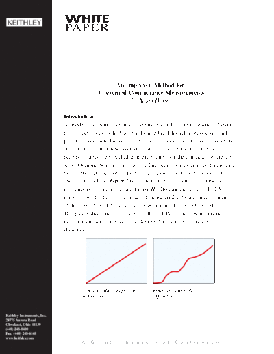
the electrical characteristics. In the macroscopic world, conductors may have
obeyed Ohm's Law (Figure 1a), but in the nanoscale, Ohm's definition of
resistance is no longer relevant (Figure 1b). Because the slope of the I-V curve
is no longer a fundamental constant of the material, a detailed measurement
of the slope of that I-V curve at every point is needed to study nanodevices.
This plot of differential conductance (dG = dI/dV) is the most important
measurement made on small scale devices, but presents a unique set of
challenges.
Figure 1a. Macroscopic scale Figure 1b. Nanoscale
(Classical) (Quantum)
Keithley Instruments, Inc.
28775 Aurora Road
Cleveland, Ohio 44139
(440) 248-0400
Fax: (440) 248-6168
www.keithley.com
A G r e a t e r M e a s u r e o f C o n f i d e n c e
Who Uses Differential Conductance?
Differential conductance measurements are performed in many areas of research, though
sometimes under different names. When used to measure the electron energy structure of
small devices such as quantum dots, nanoparticles, or artificial atoms, it is sometimes referred
to as electron energy spectroscopy. When used to perform non-contact measurements on
surfaces within a scanning tunneling microscope, it may be called tunneling spectroscopy.
When studying ultra-small semiconductor structures or nanotubes with semiconducting
properties, it might be called a density of states measurement. Still other researchers refer
to it more mathematically, as the derivative of the I-V curve, or simply dI/dV or G. It can
be used to understand conduction phenomenon in cryogenic environments or to observe
and predict the conditions when tunneling is more likely to occur. A few examples of the
device types that can be studied this way are Schottky diodes, tunnel diodes, and single-
electron transistors. The fundamental reason differential conductance is interesting is that the
conductance reaches a maximum at voltages (or more precisely, at electron energies in eV)
at which the electrons are most active. This explains the common use of the name energy
spectroscopy. This is also why dI/dV is directly proportional to the density of states and is
the most direct way to measure it.
Existing Methods of Performing Differential Conductance
While there is no standardized technique to obtain differential conductance, almost all
approaches have followed one of two methods:
(1) Perform a current-voltage sweep (I-V curve) and take the mathematical derivative,
or
(2) Use an AC technique of applying a sinusoidal signal superimposed on a DC bias
to the sample. Then use a lock-in amplifier to obtain the AC voltage across and the
AC current through the DUT (device under test).
I-V Technique
The I-V sweep technique has the advantage that it is easier to set up and control. It only
requires one source and one measurement instrument, which makes it relatively easy to
coordinate and control. The fundamental problem is that even a small amount of noise
becomes a large noise when the measurements are differentiated.
A G r e a t e r M e a s u r e o f C o n f i d e n c e
Figure 2a. I-V curve Figure 2b. Differentiated I-V Figure 2c. 100 curves, averaged
curve together
Figure 2a shows an I-V curve, a series of sourced and measured values (V1, I1), (V2,
I2), etc. Several techniques can be used to differentiate this data, but the simplest and most
common uses the slope between every pair of consecutive data points. For example, the first
point in the differential conductance curve would be (I2◦ Jabse Service Manual Search 2026 ◦ Jabse Pravopis ◦ onTap.bg ◦ Other service manual resources online : Fixya ◦ eServiceinfo