Service Manuals, User Guides, Schematic Diagrams or docs for : Keithley Appnotes 2951_Test_Structure_Design

<< Back | Home

Most service manuals and schematics are PDF files, so You will need Adobre Acrobat Reader to view : Acrobat Download Some of the files are DjVu format. Readers and resources available here : DjVu Resources
For the compressed files, most common are zip and rar. Please, extract files with Your favorite compression software ( WinZip, WinRAR ... ) before viewing. If a document has multiple parts, You should download all, before extracting.
Good luck. Repair on Your own risk. Make sure You know what You are doing.


Image preview - the first page of the document
2951_Test_Structure_Design


>> Download 2951_Test_Structure_Design documenatation <<

Text preview - extract from the document
                                        A    GREAT ER   M EA SU R E             O F    C O N F I D E N C E                     probe pads that connect to more than one
                                                                                                                               device under test (DUT). The most frequent
                                                                                                                               application for common pads is to connect
                                                                                                                               the source terminals together for a set of
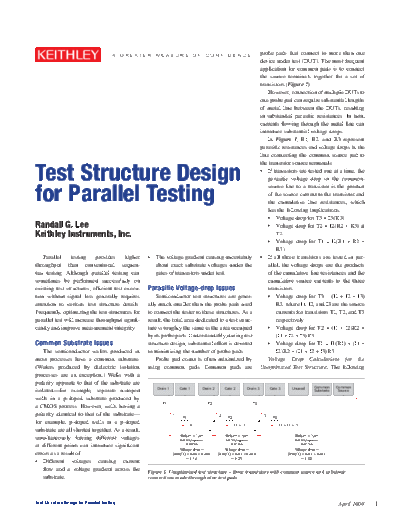
                                                                                                                               transistors (Figure 1).
                                                                                                                                   However, connection of multiple DUTs to
                                                                                                                               one probe pad can require substantial lengths
                                                                                                                               of metal line between the DUTs, resulting
                                                                                                                               in substantial parasitic resistances. In turn,
                                                                                                                               currents flowing through the metal line can
                                                                                                                               introduce substantial voltage drops.
                                                                                                                                   In Figure 1, R1, R2, and R3 represent
                                                                                                                               parasitic resistances and voltage drops in the
                                                                                                                               line connecting the common source pad to


Test Structure Design
                                                                                                                               the transistor source terminals:


◦ Jabse Service Manual Search 2024 ◦ Jabse PravopisonTap.bg ◦ Other service manual resources online : FixyaeServiceinfo