Service Manuals, User Guides, Schematic Diagrams or docs for : Keithley KPCI KPCI1802HC_RevA_DocSpec
<< Back | HomeMost service manuals and schematics are PDF files, so You will need Adobre Acrobat Reader to view : Acrobat Download Some of the files are DjVu format. Readers and resources available here : DjVu Resources
For the compressed files, most common are zip and rar. Please, extract files with Your favorite compression software ( WinZip, WinRAR ... ) before viewing. If a document has multiple parts, You should download all, before extracting.
Good luck. Repair on Your own risk. Make sure You know what You are doing.
Image preview - the first page of the document
>> Download KPCI1802HC_RevA_DocSpec documenatation <<
Text preview - extract from the document
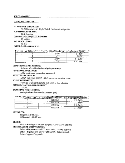
 KPCI-1802HC

 ANALOG       INPUTS
  NUMBER OF CHANNELS:
         32 Differential or 64 Single Ended; Software Configurable
 A/D FIFO BUFFER SIZE:
        2048 Samples
 CHANNEL GAIN QUEUE LENGTH:
        64 Entries
 A/D RESOLUTION:
         12 Bits
 INPUT GAIN AND RANGE:


INPUT RANGE SELECTION:
        Software selectable via channel gain queue entry
INPUT OVERVOLTAGE:
        f15V continuous, powered or unpowered.
INPUT BIAS CURRENT
       f4OnA maximum @25'C; f60nA max. over operating range,
INPUT IMPEDANCE;
       >lOOMQ or greater in parallel with 90pF or less, all gains.
SINGLE CHANNEL THROUGHPUT:
       333kS/s.
SCANNING THROUGHPUT:
       (multiple channels scanned at the same gain)


LINEARITY:
       Integral: il LSB Max.
       Differential: fl LSB Max.

ERROR:
      *0.02% Reading *lLSB max. for gains < 250, @25"C (typical)
TEMPERATURE       COEFFICIENTS:
      Offset - Unipolar: f10 pV/"C * (14 pV/T + Gain) (typical)
      Offset-Bipolar:   f10 pV/"C * (12 pV/"C + Gain) (typical)
      Gain: *20ppm/"C (typical)
Note: Accuracies and r.m.s. calculations are based on an average of 5000 samples. Add noise to get maximum uncertainty
of a single sample. "FSR" = "Full Scale Range". "RDG" = "Reading".

COMMON        MODE REJECTION              (TYPICAL):
     Gain = 1; 74dB DC - 60 Hz
     Gain = 2,4; 79dB DC - 60 Hz
     Gain = 8: 84dB DC - 60 Hz
DATA TRANSFER            MODES:
     DMA (PC1 Bus Master), Interrupt (Target-mode tmnsfer), Polled (Target-mode transfer)
ANALOG        OUTPUTS

NUMBER OF CHANNELS:
        TWO
RESOLUTION:
         12 Bits
RANGE:
       LtIOV
ACCURACY:
       * 5mV, typical into High Impedance; Output impedance = 4 Ohms.
OUTPUT CURRENT:
       f 5 mA max.
MAXIMIJM     CAPACITIVE     LOAD:
        IOOkF
DATA TRANSFER MODES:
       DMA (PC1 Bus Master), Interrupt (Target-mode transfer), Polled (Target-mode transfer)
D/A FIFO BUFFER SIZE:
        16 Samples

CLOCK/TIMER
INTERNAL PACER CLOCK RATE:
       333 kHz, max.
       0.0012 Hz, min.
EXTERNAL PACER CLOCK RATE:
       333kHz, max.
EXTERNAL PACER CLOCK PULSE WIDTH:
       10 ns, min.
BURST CLOCK RATE:
       333 kHz, max.
TRIGGER:
      External digital; pre, post, about modes
      Internal sofhvare; start, stop, pre, post, about modes.
EXTERNAL TRIGGER PULSE WIDTH:
       IOns, min.
DIGITAL      I/O

INPUT BITS:
       4; TWO share connector pins for external pacer and trigger.
INPUT LOW:
      v,, = 0.8 V max.; I,, = -0SmA max.
INPUT HIGH:
       V,, = 2.0 V min.; I,,, = -350pA max.
OUTPUT BITS:
      Eight, with strobe.
OUTPUT LOW:
      V,, = 0.5 V max.; I,, = 4 mA max.
OUTPUT HIGH:
      V,, = 2.7 V min.; I,, = -4OOpA max.
DOSTRB PULSE WIDTH:
      300nseq typ.; Data latched on rising edge.
DATA TRANSFER MODE:
      Target mode.

POWER

POWER INPUT:
     +5 V; 430mA typ., 870mA max.
     +12 V; 300mA typ., 450 mA max.
POWER OUTPUT:
     5 V; l.OA max. (May also be limited by computer or bus capability)
     f15 V; 30mA max.

ENVIRONMENT

TEMPERATURE, OPERATING:
       0
◦ Jabse Service Manual Search 2026 ◦ Jabse Pravopis ◦ onTap.bg ◦ Other service manual resources online : Fixya ◦ eServiceinfo