Service Manuals, User Guides, Schematic Diagrams or docs for : Keithley 2001 ds 2N4392_TG-128-1

<< Back | Home

Most service manuals and schematics are PDF files, so You will need Adobre Acrobat Reader to view : Acrobat Download Some of the files are DjVu format. Readers and resources available here : DjVu Resources
For the compressed files, most common are zip and rar. Please, extract files with Your favorite compression software ( WinZip, WinRAR ... ) before viewing. If a document has multiple parts, You should download all, before extracting.
Good luck. Repair on Your own risk. Make sure You know what You are doing.


Image preview - the first page of the document
2N4392_TG-128-1


>> Download 2N4392_TG-128-1 documenatation <<

Text preview - extract from the document
Siliconix                                                            2N/PN/SST4391 Series
N Channel JFETs
                                                                         2N4391              PN4391               SST4391
                                                                         2N4392              PN4392               SST4392
                                                                         2N4393              PN4393               SST4393
Product Summary
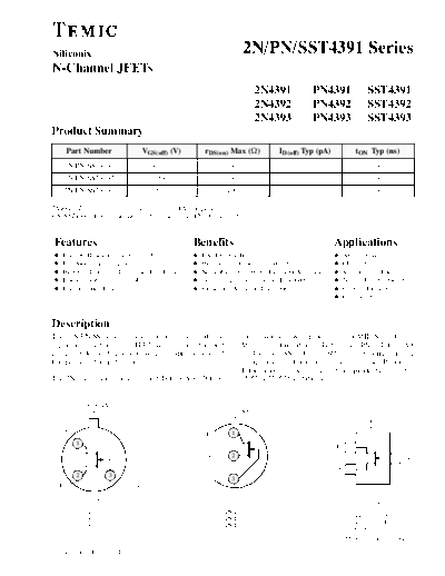
        Part Number               VGS(off) (V)          rDS(on) Max (W)          ID(off) Typ (pA)             tON Typ (ns)
    2N/PN/SST4391                  -4 to -10                    30                       5                           4
    2N/PN/SST4392                   -2 to -5                    60                       5                           4
    2N/PN/SST4393                  -0.5 to -3                  100                       5                           4

2N4391, For applications information see AN104, page 21.
PN/SST4393, For applications information see AN106, page 28.


Features                                           Benefits                                         Applications
D   Low On Resistance: 4391<30 W                   D   Low Error Voltage                            D   Analog Switches
D   Fast Switching tON: 4 ns                       D   High Speed Analog Circuit Performance        D   Choppers
D   High Off Isolation: ID(off) with Low Leakage   D   Negligible Off Error," Excellent Accuracy    D   Sample and Hold
D   Low Capacitance: < 3.5 pF                      D   Good Frequency Response, Low Glitches        D   Normally On" Switches
D   Low Insertion Loss                             D   Eliminates Additional Buffering              D   Current Limiters
                                                                                                    D   Commutators


Description
The 2N/PN/SST4391 series features many of the                        can is available with processing per MIL S 19500 (see
superior characteristics of JFETs which make it a good               Military Information). Both the PN, TO 226AA
choice for demanding analog switching applications and               (TO 92), and SST, TO 236 (SOT 23), series are available
for specialized amplifier circuits.                                  in tape and reel for automated assembly (see Packaging
                                                                     Information). For similar dual products, see the
The 2N series hermetically sealed TO 206AA (TO 18)                   2N5564/5565/5566 data sheet.


              TO 206AA
               (TO 18)                                        TO 226AA
                                                               (TO 92)
                                                                                                                 TO 236
                                                                                                                (SOT 23)
    S                                                            1
                                                        D
          1
                                                                                                    D     1
                                                         S       2                                                         3   G
                                                                                                    S     2
          2              3                              G        3
    D                        G and Case

              Top View                                        Top View
                                                                                                                Top View
               2N4391                                          PN4391
                                                                                                              SST4391 (CA)*
               2N4392                                          PN4392
                                                                                                              SST4392 (CB)*
               2N4393                                          PN4393
                                                                                                              SST4393 (CC)*
                                                                                                        *Marking Code for TO 236

P-37410--Rev. D (07/04/94)                                                                                                     1
2N/PN/SST4391 Series                                                                                                                                                Siliconix

Absolute Maximum Ratings
Gate Drain, Gate Source Voltage: (2N/PN Prefixes) . . . . . . . -40 V                                     Operating Junction Temperature : (2N Prefix) . . . . . -55 to 200 _C
                                 (SST Prefix) . . . . . . . . . . . -35 V                                                                  (PN/SST Prefixes) -55 to 150 _C
Gate Current . . . . . . . . . . . . . . . . . . . . . . . . . . . . . . . . . . . . . . . . . 50 mA      Power Dissipation :    (2N Prefix)a . . . . . . . . . (TC = 25_C) 1800 mW
                                                                                                                                 (PN/SST Prefixes)b . . . . . . . . . . . . . . . 350 mW
Lead Temperature . . . . . . . . . . . . . . . . . . . . . . . . . . . . . . . . . . . . 300 _C
                                                                                                          Notes
Storage Temperature : (2N Prefix) . . . . . . . . . . . . . . . -65 to 200 _C                             a. Derate 10 mW/_C above 25_C
                      (PN/SST Prefixes) . . . . . . . . . -55 to 150 _C                                   b. Derate 2.8 mW/_C above 25_C


 Specificationsa
                                                                                                                                             Limits
                                                                                                                              4391              4392               4393

            Parameter                       Symbol                         Test Conditions                      Typb Min        Max      Min       Max       Min      Max       Unit

 Static

 Gate Source                                                           IG = -1 mA                      2N/PN    -55     -40               -40                -40
 Breakdown V l
           Voltage                         V(BR)GSS
 B kd                                                                   VDS = 0 V                       SST     -55     -35               -35                -35
                                                                                                                                                                                  V
 Gate Source                                                  VDS = 20 V              2N/PN: ID = 1 nA
                                            VGS(off)                                                                    -4       -10      -2        -5       -0.5
                                                                                                                                                             -0 5      -3
 Cutoff Voltage
 C ff V l                                                     VDS = 15 V               SST: ID = 10 nA
                                                                                                        2N              50       150       25          75      5          30
 Saturation D i
 S      i Drain           Currentc
                          C                    IDSS            VDS = 20 V, VGS = 0 V
                                                                        V                               PN              50       150       25       100        5          60     mA
                                                                                                                                                                                  A
                                                                                                        SST             50                 25                  5
                                                                                                       2N/SST    -5             -100               -100               -100
                                                             VGS = -20 V VDS = 0 V
                                                                       V,                                                                                                        pA
                                                                                                        PN       -5             -1000             -1000              -1000
 G    Reverse C
 Gate R       Current                          IGSS                                    2N: TA = 150_C           -13             -200               -200               -200
                                                                                       PN: TA = 100_C            -1             -200               -200               -200       nA
                                                                                                                                                                                  A
                                                                                      SST: TA = 125_C            -3
 Gate Operating Current                         IG                   VDG = 15 V, ID = 10 mA                      -5
                                                                                       2N: VGS = -5 V            5                                                     100
                                                                                                                                                                                 pA
                                                                                                                                                                                  A
                                                                                       2N: VGS = -7 V            5                                  100
                                                                                      2N: VGS = -12 V            5               100
                                                              VDS = 20 V
                                                                                       PN: VGS = -5 V           0.005                                                     1
                                                                                       PN: VGS = -7 V           0.005                                  1                         nA
                                                                                                                                                                                  A
                                                                                      PN: VGS = -12 V           0.005                1
                                                                 SST VDS = 10 V, VGS = -10 V                     5               100                100                100       pA
 Drain Cutoff C
 D i C ff Current                             ID(off)                                  2N: VGS = -5 V            13                                                    200
                                                              VDS = 20 V
                                                                                       2N: VGS = -7 V            13                                 200
                                                              TA = 150_C
                                                                   150 C
                                                                                      2N: VGS = -12 V            13              200
                                                                                       PN: VGS = -5 V            1                                                     200
                                                                                                                                                                                 nA
                                                                                                                                                                                  A
                                                             VDS = 20 V
                                                                                       PN: VGS = -7 V            1                                  200
                                                             TA = 100_C
                                                                  100 C
                                                                                      PN: VGS = -12 V            1               200
                                                              VDS = 10 V
                                                                                     SST: VGS = -10 V            3
                                                              TA = 125_C
                                                                                               ID = 3 mA        0.25                                                   0.4
 D i S        On Voltage
 Drain Source O V l                         VDS(on)               VGS = 0 V                    ID = 6 mA         0.3                                0.4                           V
                                                                                              ID = 12 mA        0.35             0.4

 2                                                                                                                                                     P-37410--Rev. D (07/04/94)
Siliconix                                                               2N/PN/SST4391 Series
 Specificationsa
                                                                                                       Limits
                                                                                         4391          4392          4393

        Parameter            Symbol              Test Conditions             Typb Min          Max   Min   Max     Min   Max     Unit

 Static (Cont'd)
 Drain Source
                             rDS(on)          VGS = 0 V, ID = 1 mA                              30            60         100      W
 On Resistance

 Gate Source                                   IG = 1 mA              2N      0.7               1             1             1
                             VGS(F)                                                                                               V
 Forward V l
 F     d Voltage                               VDS = 0 V           PN/SST     0.7

 Dynamic
 Common Source
                               gfs                                             6                                                 mS
 ForwardTransconductance
                                         VDS = 20 V, ID = 1 mA f = 1 kHz
                                                  V         mA,
 Common Source
                               gos                                             25                                                mS
 Output Conductance
 Drain Source
                             rDS(on)     VGS = 0 V, ID = 0 mA , f = 1 kHz                       30            60         100      W
 On Resistance
                                                                      2N       12               14            14            14
 Common Source                           VDS = 20 V, VGS = 0 V
                                                  V
                               Ciss                                   PN       12               16            16            16
 Input Capacitance                            f = 1 MHz
                                                                      SST      13
                                                         2N: VGS = -5 V       3.3                                        3.5
                                                         2N: VGS = -7 V       3.2                          3.5
                                                        2N: VGS = -12 V       2.8              3.5
                                                                                                                                 pF
                                                                                                                                  F
                                                         PN: VGS = -5 V       3.5                                           5
 Common S
 C         Source R
                  Reverse                VDS = 0 V
                               Crss                      PN: VGS = -7 V       3.4                             5
 Transfer Capacitance                    f = 1 MHz
                                                        PN: VGS = -12 V       3.0               5
                                                        SST: VGS = -5 V       3.6
                                                        SST: VGS = -7 V       3.5
                                                        SST: VGS = -12 V      3.1
 Equivalent Input                            VDS = 10 V, ID = 10 mA                                                              nV/
                                en                                             3
 Noise Voltage                                     f = 1 kHz                                                                     Hz

 Switching
                                                                    2N/PN      2                15            15            15
                              td(on)
                                                                      SST      2
 Turn O Ti
 T    On Time
                                                                    2N/PN      2                5             5             5
                                tr
                                              VDD = 10 V              SST      2
                                             VGS(H) = 0 V                                                                         ns
                                          See Switching Circuit     2N/PN      6                20            35            50
                              td(off)
                                                                      SST      6
 Turn Off Ti
 T        Time
                                                                    2N/PN      13               15            20            30
                                tf
                                                                      SST      13

Notes
a. TA = 25_C unless otherwise noted.                                                                                              NCB
b. Typical values are for DESIGN AID ONLY, not guaranteed nor subject to production testing.
c. Pulse test: PW v300 ms duty cycle v3%.


P-37410--Rev. D (07/04/94)                                                                                                         3
2N/PN/SST4391 Series                                                                                                                                                                                                                                                 Siliconix
     Typical Characteristics
                                                         On Resistance and Drain Current
                                                          vs. Gate Source Cutoff Voltage                                                                                                                                    On Resistance vs. Drain Current
                                             100                                                                   200                                                                                        100
rDS(on) - Drain Source On Resistance ( W )


                                                                                                                                                                 rDS(on) - Drain Source On Resistance ( W )
                                                                rDS @ ID = 1 mA, VGS = 0 V                                                                                                                               TA = 25_C


                                                                                                                         I DSS - Saturation Drain Current (mA)
                                                                IDSS @ VDS = 20 V, VGS = 0 V
                                              80                                                                   160                                                                                         80


                                                                                             IDSS                                                                                                                       VGS(off) = -2 V
                                              60             rDS                                                   120                                                                                         60


                                              40                                                                   80                                                                                          40
                                                                                                                                                                                                                                    -4 V


                                              20                                                                   40                                                                                          20                   -8 V


                                               0                                                                0                                                                                               0
                                                   0       -2             -4          -6            -8       -10                                                                                                    1                           10                       100
                                                       VGS(off) - Gate Source Cutoff Voltage (V)                                                                                                                                   ID - Drain Current (mA)


                                                          On Resistance vs. Temperature                                                                                                                                              Turn On Switching
                                             200                                                                                                                                                                5
                                                       ID = 1 mA                                                                                                                                                                   tr approximately independent of ID
rDS(on) - Drain Source On Resistance ( W )


                                                       rDS changes X 0.7%/_C                                                                                                                                                       VDD = 5 V, RG = 50 W
                                             160                                                                                                                                                                4                  VGS(L) = -10 V
                                                                                                                                                                  Switching Time (ns)


                                             120                                                                                                                                                                3
                                                                                     VGS(off) = -2 V                                                                                                                                          td(on) @
                                                                                                                                                                                                                                            ID = 12 mA
                                              80                                                                                                                                                                2
                                                                                                    -4 V
                                                                                                                                                                                                                         td(on) @
                                              40                                                    -8 V                                                                                                        1       ID = 3 mA
                                                                                                                                                                                                                                                                  tr

                                               0                                                                                                                                                                0
                                                   -55 -35 -15        5        25   45       65     85 105   125                                                                                                    0         -2           -4        -6           -8    -10
                                                                   TA - Temperature (_C)                                                                                                                                 VGS(off) - Gate Source Cutoff Voltage (V)


                                                                    Turn Off Switching                                                                                                                                    Capacitance vs. Gate Source Voltage
                                             30                                                                                                                                                                30
                                                       td(off) independent of device VGS(off)                                                                                                                             f = 1 MHz
                                                       VDD = 5 V, VGS(L) = -10 V                                                                                                                                          VDS = 0 V
                                             24                                                                                                                                                                24
Switching Time (ns)


                                                                                                                                                                   Capacitance (pF)


                                             18                                     VGS(off) = -2 V                                                                                                            18


                                                                               tf
                                             12                                                                                                                                                                12
                                                         td(off)
                                                                                                                                                                                                                                                           Ciss
                                              6                                                                                                                                                                 6
                                                        VGS(off) = -8 V                                                                                                                                                                                       Crss

                                              0                                                                                                                                                                 0
                                                   0        2             4              6           8        10                                                                                                    0         -4           -8        -12          -16   -20
                                                                   ID - Drain Current (mA)                                                                                                                                    VGS - Gate Source Voltage (V)

                 4                                                                                                                                                                                                                                   P-37410--Rev. D (07/04/94)
                   Siliconix                                                                                    2N/PN/SST4391 Series
               Typical Characteristics (Cont'd)
                                                                                                                                                   Forward Transconductance and Output onductance
                                                     Noise Voltage vs. Frequency                                                                            vs. Gate Source Cutoff Voltage*
                                   100                                                                                                             50                                                         500
                                                                                                                                                               gfs and gos @ VDS = 20 V


                                                                                                           g fs - Forward Transconductance (mS)
                                                VDS = 10 V
                                                                                                                                                               VGS = 0 V, f = 1 kHz
en - Noise Voltage (nV /  Hz)


                                                                                                                                                   40                                                         400


                                                                                                                                                                                                                      g os - Output Conductance (mS)
                                                                                                                                                   30                      gfs            gos                 200
                                    10
                                                                  ID = 1 mA
                                                                                                                                                   20                                                         200


                                                         ID = 10 mA                                                                                10                                                         100


                                     1                                                                                                              0                                                         0
                                          10             100           1k           10 k           100 k                                                 0          -2           -4       -6          -8   -10
                                                               f - Frequency (Hz)                                                                              VGS(off) - Gate Source Cutoff Voltage (V)


                                                          Gate Leakage Current                                                                                    Common Gate Input Admittance
                                10 nA                                                                                                             100
                                                                              IGSS @ 125_C
                                                                                                                                                               VDG = 10 V
                                                                    ID = 10 mA                                                                                 ID = 10 mA
                                                 TA = 125_C                                                                                                                             gig
                                 1 nA                                                                                                                          TA = 25_C
  I G - Gate Leakage


                                                                                                                                                   10
                                100 pA                                    1 mA
                                                                                        1 mA                                                                                      big
                                                                                                           (mS)


                                10 pA                            10 mA            IGSS @ 25_C
                                                 TA = 25_C                                                                                          1

                                 1 pA

                                                                                 IG(on) @ ID
                                0.1 pA                                                                                                            0.1
                                          0          6            12        18         24           30                                                   100             200                    500        1000

                                                    VDG - Drain Gate Voltage (V)                                                                                           f - Frequency (MHz)


                                                 Common Gate Forward Admittance                                                                                  Common Gate Reverse Admittance
                                   100                                                                                                             10
                                                VDG = 10 V                                                                                                     VDG = 10 V
                                                ID = 10 mA                                                                                                     ID = 10 mA
                                                TA = 25_C                                                                                                      TA = 25_C
                                                                   -gfg                bfg
                                                                                                                                                   1.0                -brg
                                    10
                                                                                             gfg
   (mS)


                                                                                                           (mS)


                                                                                                                                                                    -grg
                                                                                                                                                                                           +grg

                                     1                                                                                                             0.1


                                    0.1                                                                                                           0.01
                                          100              200                   500               1000                                               100                200                   500         1000
                                                           f - Frequency (MHz)                                                                                             f - Frequency (MHz)

                     P-37410--Rev. D (07/04/94)                                                                                                                                                                   5
2N/PN/SST4391 Series                                                                                                                                                                       Siliconix
Typical Characteristics (Cont'd)
                                        Common Gate Output Admittance                                                                              Transconductance vs. Drain Current
                           100                                                                                                        100
                                       VDG = 10 V                                                                                                 VGS(off) = -2 V                    VDS = 10 V


                                                                                               g fs - Forward Transconductance (mS)
                                       ID = 10 mA                                                                                                                                    f = 1 kHz
                                       TA = 25_C
                                                                      bog
                            10                                                                                                                                                    TA = -55_C
                                                                                                                                                                        25_C
                                                                      gog
(mS)


                                                                                                                                       10


                             1                                                                                                                                                  125_C


                           0.1                                                                                                          1
                                 100              200                 500               1000                                                0.1                          1.0                          10
                                                  f - Frequency (MHz)                                                                                      ID - Drain Current (mA)


                                                 Output Characteristics                                                                                   Transfer Characteristics
                           100                                                                                                        100
                                       VGS(off) = -4 V                                                                                              VGS(off) = -4 V                  VDS = 20 V

                            80                                                                                                         80
I D - Drain Current (mA)


                                                                                               I D - Drain Current (mA)


                                                                                                                                                     TA = -55_C

                            60                                              VGS = 0 V                                                  60
                                                                                                                                                   25_C
                                                                              -0.5 V
                            40                                                -1.0 V                                                   40

                                                                              -1.5 V
                            20                                                -2.0 V                                                   20
                                                                                                                                                     125_C
                                                                              -2.5 V
                             0                                                                                                          0
                                 0          2           4         6            8         10                                                  0        -1           -2           -3         -4        -5
                                           VDS - Drain Source Voltage (V)                                                                              VGS - Gate Source Voltage (V)


Switching Time Test Circuit
                                                                                                                                                                                               VDD
                                                4391            4392               4393
              VGS(L)                         -12 V              -7 V               -5 V
                                                                                                                                                                                                     RL
              RL*                               800 W          1600 W              3000 W
              ID(on)                            12 mA           6 mA               3 mA
                                                                                                                                                                                                           OU
              *Non inductive                                                                                                           VGS(H)
                                 Input Pulse                      Sampling Scope               VGS(L)
              Rise Time < 1 ns                              Rise Time 0.4 ns
              Fall Time < 1 ns                              Input Resistance 10 MW
                                                                                                                                                                          1 kW          51 W
              Pulse Width 100 ns                            Input Capacitance 1.5 pF
              PRF 1 MHz
              See Typical Characteristics curves for changes.                                                                                               VIN
                                                                                                                                                           Scope          51 W


6                                                                                                                                                                              P-37410--Rev. D (07/04/94)


◦ Jabse Service Manual Search 2024 ◦ Jabse PravopisonTap.bg ◦ Other service manual resources online : FixyaeServiceinfo