Service Manuals, User Guides, Schematic Diagrams or docs for : Keithley 2001 ds TP0610
<< Back | HomeMost service manuals and schematics are PDF files, so You will need Adobre Acrobat Reader to view : Acrobat Download Some of the files are DjVu format. Readers and resources available here : DjVu Resources
For the compressed files, most common are zip and rar. Please, extract files with Your favorite compression software ( WinZip, WinRAR ... ) before viewing. If a document has multiple parts, You should download all, before extracting.
Good luck. Repair on Your own risk. Make sure You know what You are doing.
Image preview - the first page of the document
>> Download TP0610 documenatation <<
Text preview - extract from the document
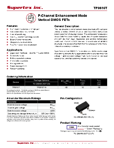
Supertex inc.                                                                                                                              TP0610T

                                                       P-Channel Enhancement Mode
                                                       Vertical DMOS FETs
Features                                                                            General Description
     High input impedance and high gain                                             This low threshold enhancement-mode (normally-off) transistor
     Low power drive requirement                                                    utilizes a vertical DMOS structure and Supertex's well-proven
     Ease of paralleling                                                            silicon-gate manufacturing process. This combination produces a
     Low CISS and fast switching speeds                                             device with the power handling capabilities of bipolar transistors
     Excellent thermal stability                                                    and with the high input impedance and positive temperature
     Integral source-drain diode                                                    coefficient inherent in MOS devices. Characteristic of all MOS
                                                                                    structures, this device is free from thermal runaway and thermally-
     Free from secondary breakdown
                                                                                    induced secondary breakdown.

Applications                                                                        Supertex's vertical DMOS FETs are ideally suited to a wide range
     Logic level interfaces - ideal for TTL and CMOS                                of switching and amplifying applications where very low threshold
     Solid state relays                                                             voltage, high breakdown voltage, high input impedance, low input
     Battery operated systems                                                       capacitance, and fast switching speeds are desired.
     Photo voltaic systems
     Analog switches
     Power management
     Telecom switches


Ordering Information
                                                Package Options                                                         RDS(ON)                  ID(ON)
                                                                                            BVDSS/BVDGS
          Device                                                                                                        (max)                    (min)
                                              TO-236AB (SOT-23)                                   (V)
                                                                                                                         ()                      (mA)
         TP0610T                                     TP0610T-G                                   -60                        10                    -50
For packaged products, -G indicates package is RoHS compliant (`Green').
Consult factory for die / wafer form part numbers.
Refer to Die Specification VF21 for layout and dimensions.


Absolute Maximum Ratings                                                                   Pin Configuration
 Parameter                                                                  Value
                                                                                                               DRAIN
 Drain-to-source voltage                                                     BVDSS
 Drain-to-gate voltage                                                      BVDGS
 Gate-to-source voltage
◦ Jabse Service Manual Search 2026 ◦ Jabse Pravopis ◦ onTap.bg ◦ Other service manual resources online : Fixya ◦ eServiceinfo