Service Manuals, User Guides, Schematic Diagrams or docs for : Keithley 213 213RevB_DocSpec
<< Back | HomeMost service manuals and schematics are PDF files, so You will need Adobre Acrobat Reader to view : Acrobat Download Some of the files are DjVu format. Readers and resources available here : DjVu Resources
For the compressed files, most common are zip and rar. Please, extract files with Your favorite compression software ( WinZip, WinRAR ... ) before viewing. If a document has multiple parts, You should download all, before extracting.
Good luck. Repair on Your own risk. Make sure You know what You are doing.
Image preview - the first page of the document
>> Download 213RevB_DocSpec documenatation <<
Text preview - extract from the document
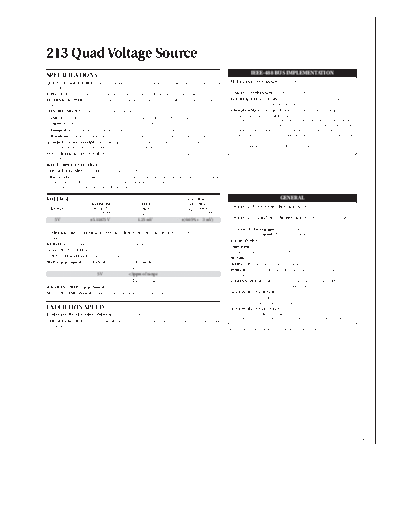
213 Quad Voltage Source
SPECIFICATIONS                                                                                                   IEEE-488 BUS IMPLEMENTATION
QUAD VOLTAGE SOURCE: Sources voltage from four independent, isolated ports. Includes 8-bit            MULTILINE COMMANDS: SDC, DCL, GET, UNL, UNT, SPE, SPD,
  digital I/O port.                                                                                     MTA, MLA.
FUNCTION: Can be used as a constant DC source or as a voltage waveform generator.                     UNILINE COMMANDS: IFC, REN, EOI, SRQ, ATN.
INTERNAL BUFFER: An 8192-location internal buffer is used to store values for waveform gener-         INTERFACE FUNCTIONS: SH1, AH1, T4, TE0, L4, LE0, SR1, RL0, PP0,
  ation.                                                                                                DC1, DT1, C0 (C28 during calibration), E1.
CONTROL MODES: Four control modes may be chosen by the user:                                          PROGRAMMABLE FUNCTIONS: Port select, output voltage, control
                                                                                                        mode, autorange enable, range select, waveform step interval,
  Direct: Output changes upon execution of the "V" device dependent command.
                                                                                                        number of cycles, offset calibration, gain calibration, buffer alloca-
  Indirect: Output changes after receiving an external trigger.                                         tion, buffer data, buffer location pointers, command trigger, trigger
  Stepped: Step through internal buffer, under control of external triggers.                            masking, SRQ masking, system defaults, digital output, EOI, IEEE-
  Waveform: Output voltage waveform from buffer, under control of an internal time base.                488 output terminator, IEEE-488 output format, system status out-
NUMBER OF WAVEFORM CYCLES: The number of cycles through the buffer in the Waveform                      put, system test, error query.
  Control Mode is user selectable, 1 to 65535 or continuous.                                          IEEE-488 address is set manually from the rear panel.
SYNCHRONIZATION OF PORTS: The ports can be forced to execute their voltage waveforms in a
  synchronized manner.
WAVEFORM STEP INTERVAL: 1ms to 65535ms.
TRIGGER AND SRQ: IEEE-488 bus or rear panel DB-25.
DIGITAL I/O: 8 TTL compatible level sensitive inputs. 8 outputs, internally selectable TTL compat-
  ible or open collector with 100mA drive and capable of withstanding 50V (for driving relays or
  other devices from an external voltage supply).

VOLTAGE                                                                        ACCURACY                                           GENERAL
                        MAXIMUM                      STEP                        18
◦ Jabse Service Manual Search 2026 ◦ Jabse Pravopis ◦ onTap.bg ◦ Other service manual resources online : Fixya ◦ eServiceinfo