Service Manuals, User Guides, Schematic Diagrams or docs for : Kenwood Radios NXR-800_K4_TA
<< Back | HomeMost service manuals and schematics are PDF files, so You will need Adobre Acrobat Reader to view : Acrobat Download Some of the files are DjVu format. Readers and resources available here : DjVu Resources
For the compressed files, most common are zip and rar. Please, extract files with Your favorite compression software ( WinZip, WinRAR ... ) before viewing. If a document has multiple parts, You should download all, before extracting.
Good luck. Repair on Your own risk. Make sure You know what You are doing.
Image preview - the first page of the document
>> Download NXR-800_K4_TA documenatation <<
Text preview - extract from the document
KENWOOD Confidential
24/Sep/2009
Measuring NXR-800 K4
1 Power up procedure
1.1 Turning on
NXR-800 has no power switch. It operates by ON/OFF of an external power-supply unit. The
power cable of the attachment must be both connected with the power-supply unit and NXR-800.
The power-supply unit with the ON/OFF function of the output voltage is recommended. After
the output voltage of the power-supply unit is set to a necessary voltage, turned on the output
voltage of the power-supply unit.
Switch existing in the volume knob on front panel of NXR-800 controls audio output ON/OFF,
not a power switch.
When the power supply is turned on, NXR-800 begins CPU start sequence. LED of the front
panel begins blinking. LED lights when about one minute passes. All afterwards, 17segments
LED begins blinking. When about one minute passes, channel information is displayed in 17
segments LED. At this point, the operation preparation of NXR-800 is completed.
OCXO is built into NXR-800. Built-in OCXO needs warm up time. General measurement should
be started 15 minutes later after the power supply turned on. Warm up for about at least 30
minutes when you execute the measurement of the frequency precision.
1.2 Until OCXO and the modulator operate normally
Built-in OCXO can be switched non-active/active. OCXO starts in active mode when the power
supply is turned on ("RPT DISABLE" Key LED lighting). Pressing the "RPT DISABLE" Key
changes OCXO Non-active/active whenever Key is pressed. ("RPT DISABLE" Key LED is off
when OCXO is in non-active mode.)
.
OCXO LED (Showing the status of a standard signal) lights green when OCXO is used. When OCXO is
not used and the internal standard signal is used, LED will be off. While using the standard signal input
Page 1
KENWOOD Confidential
24/Sep/2009
from the outside equipment, LED lights in orange.
The frequency precision is not guaranteed during 30minutes from power supply turned on. Measure it
after 30 minutes or more from the power supply turning on of OCXO (At the activated time) when you
measure the frequency stability level and the modulation characteristic, etc.
If measuring after the "RPT DSABLE" key pressed (OCXO off), wait at least 1minute after turning the
OXCO on again. This will make enough time to settle the built-in frequency of PLL.
There is no need to wait when changing the channel with 'B' or 'C' key.
1.3 About 'E3' display of 17 segments LED
"E3" display might appear to 17segment LED when "RPT DSABLE" key is turned on and off. About one
minute passes, "E3" display becomes a usual channel display as previously stated. This is normal action.
2 FPU Settings
2.1 Method of connecting FPU
Test Mode procedure.
-After CPU of NXR-800 starts, use the cross cable to connect the serial port of PC and
D-SUB9 pin connector of the front panel. The cross cable must be "Null modem cable
with full handshaking"
-Start the software of FPU.
-Select `Program/Read Data from the Repeater' from the menu. Click the `Read' in
dialog box.
-The dialog that shows progress appears. When the data reading is completed, click
`OK'.
-Check if the 17segment LED showing channel information, then select `Program/Test
Mode' from the menu.
-'PC' will be displayed in 17segment LED, and the test mode window opens.
-Click `Close' when returning to normal operation.
-All the LED will be off and on, then the channel display blinks in 17segment LED.
Afterwards channel display appears normally.
2.2 Adjustment item
NXR-800 can be adjusted from test mode window.
2.2.1 Adjustment of transmitting power
Click 'High Transmit Power' or 'Low Transmit Power' from the list, and push 'Enter'. Or, double
click the item in the list. Select the transmit frequency from the tab of Low/Center/High, and
adjust the value with slider bar.
The adjusted value is recorded in NXR-800 by clicking 'Apply All' in each tab.
Page 2
KENWOOD Confidential
24/Sep/2009
2.2.2 Maximum Deviation adjustment of analog mode
Click `Maximum Deviation (Analog)' from the list, and press 'Enter'. Or, double-click the item.
After Analog Wide/Analog Narrow is selected, use the slide bar to adjust the value.
Complete adjustment by pressing `Apply' which will record the adjusted value to NXR-800.
It is necessary to do a special procedure to adjust the digital mode. When the adjustment is
needed in a digital mode by any chance, it is necessary to readjust in Kenwood. Never adjust
the item of 'Maximum Deviation (NXDN)' and 'Deviation', if you don't know the procedure.
2.3 Sending of CW ID
NXR-800 has the function to send CW ID. It is necessary to keep sending CW ID continuously
to measure the emission mask etc. though the transmission usually ends if finished sending the
standard number of characters. The setting method when the emission mask is measured in the
Very Narrow mode is shown as follows.
2.3.1 CW ID sending method in test mode (Very Narrow measuring).
Select "Narrow" from the `Wide/Narrow' pull down menu in the Test Mode window (Narrow/Very
Narrow measurement uses common setting window). Click 'CW ID Deviation' from the list of the
adjustment item, and press 'Enter'. Or, double-click the item in the list. Check if the `Analog
Narrow' shown on the top right corner on the window, then press `Transmit' button to start the
transmission.
Narrow Deviation should be adjusted to 1 kHz. If not, use the slide bar in left to adjust the value.
2.4 Test Frequency
Test mode frequency can be selected from the prepared `Test Frequency' table. Edit this table to
change the test mode frequency.
Page 3
KENWOOD Confidential
24/Sep/2009
Select `Edit/ Test Frequency' to show Test Frequency table. (Example of K3 type below)
Add user defined frequency to the table then click 'Close' button to close the table. There should be a
warning which is meaning "Please write data before entering test mode", then press 'OK'.
Before entering test mode, select `Program/Write Data to the Repeater' from the menu to apply the fixed
data to NXR-800. Changes made in test frequency table will not be applied to NXR-800 without
procedure shown above.
Page 4
KENWOOD Confidential
24/Sep/2009
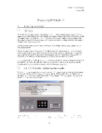
Select Program/Test Mode.
The Frequency added to the Test Frequency table can be selected from the Channel selection part on the
upper left. Channel selected here is reflected in each adjustment item.
The adjustment screen of CW ID is shown as follows. RX 422.000MHz and TX 414.725MHz of Channel
10 are displayed.
Page 5
NXR-800-K4
FOR MODEL: NXR-800
FINAL UNIT
CIRCUIT
SYMBOL PART NUMBER DESCIPTION
D4 Z5W27V SURGE ABSORBER
D5 DSM3MA1-RPB DIODE
D6 1SS355 DIODE
D7 02CZ5.6(Y)F ZENER DIODE
D9 HSB88WS DIODE
D10 HSB88WS DIODE
D11 L7091CER DIODE
D14 L7091CER DIODE
D15 L7091CER DIODE
D16 L7091CER DIODE
D19 02CZ4.7(Y)F ZENER DIODE
IC1 LTC6101BIS5-F ANALOGUE IC
IC2 NJM2904E-ZB ANALOGUE IC
IC3 TA78L05FF MOS-IC
IC4 NJM2904E-ZB ANALOGUE IC
IC5 NJM2904E-ZB ANALOGUE IC
IC6 NJM2904E-ZB ANALOGUE IC
IC7 S-8130AC MOS-IC
IC8 NJM2904E-ZB ANALOGUE IC
IC9 S24CS02AFJTBG ROM IC
IC10 RA13H3340M131 MOS-IC
IC11 NJM7808FA-ZB BI-POLAR IC
IC12 NJM7805FA-ZB BI-POLAR IC
IC15 NJM2904E-ZB ANALOGUE IC
IC701 NJM78L05UA-ZB BI-POLAR IC
IC702 LTC1046IS8 MOS-IC
IC703 TK72130CS BI-POLAR IC
Q2 SSM3K15TE(F) FET
Q3 2SA1362-F(GR) TRANSISTOR
Q4 2SJ506-E(S) FET
Q5 SSM3K15TE(F) FET
Q6 SSM3K15TE(F) FET
Q8 SSM3K15TE(F) FET
Q14 SSM3K15TE(F) FET
FOR MODEL: NXR-800
RX UNIT
CIRCUIT
SYMBOL PART NUMBER DESCIPTION
D1 HSC119 DIODE
D2 HSC119 DIODE
D3 1SV283F VARIABLE CAPACITANCE DIODE
D4 1SV283F VARIABLE CAPACITANCE DIODE
D5 1SV283F VARIABLE CAPACITANCE DIODE
D6 1SV283F VARIABLE CAPACITANCE DIODE
D7 1SV283F VARIABLE CAPACITANCE DIODE
D8 1SV283F VARIABLE CAPACITANCE DIODE
D9 JDP4P02U DIODE
D10 JDP4P02U DIODE
D11 KV1470-G VARIABLE CAPACITANCE DIODE
D12 1SV283F VARIABLE CAPACITANCE DIODE
D13 JDP4P02U DIODE
D14 JDP4P02U DIODE
D15 DAN235E DIODE
D16 DAN235E DIODE
D17 MA3J742 DIODE
D18 MA3J742 DIODE
D19 DAN235E DIODE
D20 DAN235E DIODE
D21 B30-2230-05 LED
IC4 TA75S01F-F MOS-IC
IC5 ADF4111BCP7 MOS-IC
IC6 LMC7101BIM5 MOS-IC
IC7 AD9835BRUZ MOS-IC
IC8 NJU6368PF1 MOS-IC
IC9 UPB1509GV BI-POLAR IC
IC10 TK11230CMCL-G BI-POLAR IC
IC11 ADF4111BCP7 MOS-IC
IC12 TA31137FNG MOS-IC
IC13 AD607Z BI-POLAR IC
IC14 AD8051ART ANALOGUE IC
IC15 NJM78L05UA-ZB BI-POLAR IC
IC16 NJM78L05UA-ZB BI-POLAR IC
IC17 NJM78M05DL1AZB ANALOGUE IC
IC18 NJM78M05DL1AZB ANALOGUE IC
IC19 NJM78M05DL1AZB ANALOGUE IC
IC20 NJM4558E-ZB ANALOGUE IC
IC22 XC6204B332M MOS-IC
IC23 BH2220FVM ANALOGUE IC
IC24 NJM7808FA-ZB BI-POLAR IC
IC25 NJM7808FA-ZB BI-POLAR IC
IC26 NJM2386ADL3-09 ANALOGUE IC
IC27 NJM2386ADL3-09 ANALOGUE IC
IC28 AD1582 ANALOGUE IC
IC29 NJM2732V BI-POLAR IC
IC30 AD7908BRU MOS-IC
IC31 S24CS02AFJTBG ROM IC
IC32 NJM2732V BI-POLAR IC
IC33 LMC7101BIM5 MOS-IC
IC35 LM50BIM3/NOPB MOS-IC
Q1 2SC5337 TRANSISTOR
Q2 2SC4116(BL)F TRANSISTOR
Q3 2SC4617(R) TRANSISTOR
Q4 2SC4116(BL)F TRANSISTOR
Q5 2SC4617(R) TRANSISTOR
Q6 2SC4116(BL)F TRANSISTOR
Q7 2SK2539-7 FET
Q8 2SK2539-7 FET
Q9 2SC4116(BL)F TRANSISTOR
Q10 2SC4116(BL)F TRANSISTOR
Q11 2SC4116(BL)F TRANSISTOR
Q12 2SC4617(R) TRANSISTOR
Q13 2SA1832F TRANSISTOR
Q14 SSM3K15TE(F) FET
Q15 SSM3K15TE(F) FET
Q16 2SC3356-A(R24) TRANSISTOR
Q17 2SC3356-A(R24) TRANSISTOR
Q18 RD01MUS1-T113 FET
Q19 RD01MUS1-T113 FET
Q20 RD01MUS1-T113 FET
Q21 2SC4725 TRANSISTOR
Q22 2SC4617(R) TRANSISTOR
Q23 2SC3356-A(R24) TRANSISTOR
Q24 2SK508NV(K52) FET
Q25 SSM3J01F FET
Q26 SSM3K15TE(F) FET
Q27 2SC4116(BL)F TRANSISTOR
Q28 3SK317-E FET
Q29 3SK317-E FET
Q30 2SC4617(R) TRANSISTOR
Q31 SSM3K15TE(F) FET
Q32 SSM3J01F FET
Q33 2SC4725 TRANSISTOR
Q34 2SA1832F TRANSISTOR
Q35 2SC4725 TRANSISTOR
Q36 2SC4725 TRANSISTOR
Q37 SSM3K15TE(F) FET
Q38 2SC4725 TRANSISTOR
Q39 2SC4617(R) TRANSISTOR
Q40 2SC4617(S) TRANSISTOR
Q45 SSM3K15TE(F) FET
Q50 SSM3K15TE(F) FET
Q51 SSM3K15TE(F) FET
Q52 2SJ484 FET
Q53 2SC4725 TRANSISTOR
Q55 SSM3K15TE(F) FET
Q56 SSM3K15TE(F) FET
Q57 DTA144EE TRANSISTOR
Q58 SSM3K15TE(F) FET
Q59 SSM3K15TE(F) FET
FOR MODEL: NXR-800
TX UNIT
CIRCUIT
SYMBOL PART NUMBER DESCIPTION
D101 1SV283F VARIABLE CAPACITANCE DIODE
D102 1SV283F VARIABLE CAPACITANCE DIODE
D106 1SV278F VARIABLE CAPACITANCE DIODE
D107 1SV283F VARIABLE CAPACITANCE DIODE
D108 1SV283F VARIABLE CAPACITANCE DIODE
D112 1SV278F VARIABLE CAPACITANCE DIODE
D201 HSM88AS-E DIODE
D202 B30-2230-05 LED
D301 B30-2230-05 LED
D401 HSM88AS-E DIODE
D402 HSM88AS-E DIODE
D403 HSM88AS-E DIODE
D404 JDP4P02U DIODE
D405 JDP4P02U DIODE
D406 HSC119 DIODE
D407 HSC119 DIODE
D408 HSM88AS-E DIODE
D409 CSA70-401L SURGE ABSORBER
D601 JDP4P02U DIODE
D602 JDP4P02U DIODE
D603 UDZS3.0B ZENER DIODE
D604 UDZS3.0B ZENER DIODE
D605 UDZS3.0B ZENER DIODE
D606 UDZS3.0B ZENER DIODE
D920 B30-2019-05 LED
D921 B30-2108-05 LED
D922 B30-2019-05 LED
D923 B30-2056-05 LED
D924 B30-2019-05 LED
D925 B30-2171-05 LED
D926 B30-2171-05 LED
D927 B30-2171-05 LED
D928 B30-2171-05 LED
D929 B30-2171-05 LED
D930 B30-2171-05 LED
D931 B30-2171-05 LED
D932 B30-2171-05 LED
D933 HSM88AS-E DIODE
D934 HSM88AS-E DIODE
D935 1SS355 DIODE
D936 1SS355 DIODE
D960 PSA05-11SRWA LED
D961 PSA05-11SRWA LED
IC101 LMX2352TMX/NP ANALOGUE IC
IC102 LMC7101BIM5 MOS-IC
IC104 NJM2386ADL3-09 ANALOGUE IC
IC201 NJM2904E-ZB ANALOGUE IC
IC202 AD9835BRUZ MOS-IC
IC301 NJM2732V BI-POLAR IC
IC302 NJU6368PF1 MOS-IC
IC303 ADF4001BRUZ MOS-IC
IC304 M62364FP-F MOS-IC
IC305 NJM2732V BI-POLAR IC
IC306 LMC7101BIM5 MOS-IC
IC307 NJU6368PF1 MOS-IC
IC308 NJM2732V BI-POLAR IC
IC401 LMC7101BIM5 MOS-IC
IC404 ADF4001BRUZ MOS-IC
IC405 TC75S59F-F MOS-IC
IC406 TC75S59F-F MOS-IC
IC407 NJU6368PF1 MOS-IC
IC408 TA75S01F-F MOS-IC
IC409 TA75S01F-F MOS-IC
IC601 AD9835BRUZ MOS-IC
IC602 NJU6368PF1 MOS-IC
IC603 XC6204B332M MOS-IC
IC701 BH2220FVM ANALOGUE IC
IC702 S24CS02AFJTBG ROM IC
IC703 BU4094BCFV MOS-IC
IC704 NJM78M08DL1AZB ANALOGUE IC
IC705 NJM78M05DL1AZB ANALOGUE IC
IC706 NJM78M05DL1AZB ANALOGUE IC
IC801 AD1582 ANALOGUE IC
IC802 AD5312BRM MOS-IC
IC803 AD7908BRU MOS-IC
IC804 LM50BIM3/NOPB MOS-IC
IC805 TC7SET126FU-F MOS-IC
IC806 TC7SET126FU-F MOS-IC
IC807 NJM78M05DL1AZB ANALOGUE IC
IC808 NJM7808FA-ZB BI-POLAR IC
IC809 NJM7808FA-ZB BI-POLAR IC
IC920 TC7SET126FU-F MOS-IC
IC921 TC7SET126FU-F MOS-IC
IC922 TC7SET126FU-F MOS-IC
IC923 BU4094BCFV MOS-IC
IC924 BU4094BCFV MOS-IC
IC925 BU4094BCFV MOS-IC
IC926 NJM2732V BI-POLAR IC
IC960 BU4094BCFV MOS-IC
IC961 BU4094BCFV MOS-IC
IC962 BU4094BCFV MOS-IC
IC963 BU4094BCFV MOS-IC
Q101 SSM3K15TE(F) FET
Q102 2SK2539-7 FET
Q103 2SK2539-7 FET
Q104 2SC3356-A(R24) TRANSISTOR
Q105 2SC4116(BL)F TRANSISTOR
Q106 2SC3356-A(R24) TRANSISTOR
Q107 2SC4116(BL)F TRANSISTOR
Q108 2SC4116(BL)F TRANSISTOR
Q109 2SA1832F TRANSISTOR
Q110 SSM3K15TE(F) FET
Q201 2SC3356-A(R24) TRANSISTOR
Q202 2SC5337 TRANSISTOR
Q203 RD01MUS1-T113 FET
Q204 SSM3K15TE(F) FET
Q205 SSM3J01F FET
Q206 SSM3K15TE(F) FET
Q210 SSM3K15TE(F) FET
Q211 2SC4617(R) TRANSISTOR
Q212 2SC4617(R) TRANSISTOR
Q213 2SC4617(R) TRANSISTOR
Q301 SSM3K15TE(F) FET
Q302 SSM3K15TE(F) FET
Q303 2SA1832F TRANSISTOR
Q304 2SC4617(R) TRANSISTOR
Q305 2SC4617(R) TRANSISTOR
Q307 2SC4617(R) TRANSISTOR
Q401 2SC4617(R) TRANSISTOR
Q402 2SC4617(R) TRANSISTOR
Q405 SSM3K15TE(F) FET
Q407 SSM3K15TE(F) FET
Q408 SSM3K15TE(F) FET
Q409 SSM3K15TE(F) FET
Q410 2SA1832F TRANSISTOR
Q412 2SC4617(R) TRANSISTOR
Q413 SSM3K15TE(F) FET
Q414 SSM3K15TE(F) FET
Q415 2SC4617(R) TRANSISTOR
Q416 2SC4617(R) TRANSISTOR
Q417 2SC4617(R) TRANSISTOR
Q418 2SC4617(R) TRANSISTOR
Q419 2SC4617(R) TRANSISTOR
Q420 3SK317-E FET
Q421 SSM6L05FU-F FET
Q422 RD01MUS1-T113 FET
Q423 SSM6L05FU-F FET
Q424 SSM3K15TE(F) FET
Q425 RD01MUS1-T113 FET
Q426 SSM3J01F FET
Q428 SSM3K15TE(F) FET
Q429 SSM3K15TE(F) FET
Q430 3SK317-E FET
Q431 3SK317-E FET
Q601 SSM3J01F FET
Q602 SSM3K15TE(F) FET
Q603 2SC4617(R) TRANSISTOR
Q604 SSM3K15TE(F) FET
Q605 SSM3J01F FET
Q606 2SC4617(R) TRANSISTOR
Q607 SSM3K15TE(F) FET
Q608 SSM3K15TE(F) FET
Q609 SSM3K15TE(F) FET
Q701 SSM3K15TE(F) FET
Q702 SSM3K15TE(F) FET
Q920 UMG1N TRANSISTOR
Q921 UMG1N TRANSISTOR
Q922 UMG1N TRANSISTOR
Q923 UMG1N TRANSISTOR
Q924 UMG1N TRANSISTOR
Q925 UMG1N TRANSISTOR
Q926 UMG1N TRANSISTOR
Q927 UMG1N TRANSISTOR
Q928 UMG1N TRANSISTOR
Q929 UMG1N TRANSISTOR
Q930 UMG1N TRANSISTOR
Q931 2SC4116(Y)F TRANSISTOR
Q932 2SA1586(Y)F TRANSISTOR
Q960 UMG1N TRANSISTOR
Q961 UMG1N TRANSISTOR
Q962 UMG1N TRANSISTOR
Q963 UMG1N TRANSISTOR
Q964 UMG1N TRANSISTOR
Q965 UMG1N TRANSISTOR
Q966 UMG1N TRANSISTOR
Q967 UMG1N TRANSISTOR
Q968 UMG1N TRANSISTOR
Q969 UMG1N TRANSISTOR
Q970 UMG1N TRANSISTOR
Q971 UMG1N TRANSISTOR
Q972 UMG1N TRANSISTOR
Q973 UMG1N TRANSISTOR
Q974 UMG1N TRANSISTOR
Q975 UMG1N TRANSISTOR
Q976 UMG1N TRANSISTOR
FOR MODEL: NXR-800
CONTROL UNIT
CIRCUIT
SYMBOL PART NUMBER DESCIPTION
D1 CMS05-Q DIODE
D2 CMS05-Q DIODE
D3 DA204U DIODE
D4 DA204U DIODE
D5 1SS355 DIODE
D6 02DZ18F-X ZENER DIODE
D7 DA204U DIODE
D8 DA204U DIODE
D9 DA204U DIODE
D10 DA204U DIODE
D11 DA204U DIODE
D12 1SS355 DIODE
D13 02DZ18F-X ZENER DIODE
D14 DA204U DIODE
D15 DA204U DIODE
D16 DA204U DIODE
D17 DA204U DIODE
D18 DA204U DIODE
D20 DA204U DIODE
D23 DA204U DIODE
D24 SMD185F-2 VARISTOR
D25 MINISMDC020F VARISTOR
D26 1SS388F DIODE
D28 1SS355 DIODE
D29 02DZ18F-X ZENER DIODE
D30 1SS355 DIODE
D31 02DZ18F-X ZENER DIODE
D32 1SS355 DIODE
D33 02DZ18F-X ZENER DIODE
D36 DA204U DIODE
D37 DA204U DIODE
D38 1SS388F DIODE
D39 1SS388F DIODE
IC1 BU4094BCFV MOS-IC
IC2 BU4053BCFV MOS-IC
IC3 BU4053BCFV MOS-IC
IC4 AK4550VTP MOS-IC
IC5 NJM2732V BI-POLAR IC
IC6 XC6209B332PR MOS-IC
IC7 TA75S01F-F MOS-IC
IC8 M62364FP-F MOS-IC
IC9 NJM2734V BI-POLAR IC
IC10 NJM2340RB1 MOS-IC
IC11 NJM2340RB1 MOS-IC
IC12 NJM2732V BI-POLAR IC
IC14 BU4053BCFV MOS-IC
IC15 BA33BC0FP MOS-IC
IC16 XC6209B502PR MOS-IC
IC17 AL008D90BFI02 ROM IC
IC18 XC6201P182MR MOS-IC
IC19 NJM2732V BI-POLAR IC
IC20 NJM2734V BI-POLAR IC
IC21 NJM2734V BI-POLAR IC
IC22 BU4094BCFV MOS-IC
IC23 TC7SH00FU-F MOS-IC
IC25 TC7S66FUF MOS-IC
IC27 TC7SET126FU-F MOS-IC
IC28 TC7SH126FU-F MOS-IC
IC29 LA4425A MOS-IC
IC30 TC7SH00FU-F MOS-IC
IC31 TC7MH4040FK-F MOS-IC
IC32 TC7SH126FU-F MOS-IC
IC33 TC7SH126FU-F MOS-IC
IC34 M30627FHPGP MICROPROCESSOR IC
IC35 S24CS02AFJTBG ROM IC
IC36 TC7MET541AFK MOS-IC
IC37 320VC5402PGE MICROPROCESSOR IC
IC38 TC7SET08FU-F MOS-IC
IC39 TC7SH125FU-F MOS-IC
IC40 TC7SH126FU-F MOS-IC
IC41 TC7SH08FU-F MOS-IC
IC50 TC7SH08FU-F MOS-IC
Q1 DTC114EUA TRANSISTOR
Q2 2SJ506-E(S) FET
Q3 2SJ506-E(S) FET
Q4 2SC4738F TRANSISTOR
Q5 2SC4738F TRANSISTOR
Q6 DTC363EU TRANSISTOR
Q7 DTC114EUA TRANSISTOR
Q8 DTC114EUA TRANSISTOR
Q9 2SJ506-E(S) FET
Q10 2SC4738F TRANSISTOR
Q11 2SD2114K(W) TRANSISTOR
Q12 2SC4738F TRANSISTOR
Q13 2SD2114K(W) TRANSISTOR
Q14 2SC4116(Y)F TRANSISTOR
Q15 2SA1586(Y)F TRANSISTOR
Q16 2SC4116(Y)F TRANSISTOR
Q17 2SA1586(Y)F TRANSISTOR
Q18 2SK1830F FET
Q19 HN1L02FU(F) FET
Q20 2SA1955A-F TRANSISTOR
Q21 DTC144EUA TRANSISTOR
Q22 2SA1955A-F TRANSISTOR
Q23 DTC144EUA TRANSISTOR
Q25 DTC144EUA TRANSISTOR
Q26 DTC144EUA TRANSISTOR
Q27 2SD2114K(W) TRANSISTOR
Q28 2SD2114K(W) TRANSISTOR
Q29 2SD2114K(W) TRANSISTOR
FOR MODEL: NXR-800
CONTROL UNIT
CIRCUIT
SYMBOL PART NUMBER DESCIPTION
D300 1SS388F DIODE
D301 MA2S111-F DIODE
D701 1SS388F DIODE
D702 1SS355 DIODE
IC300 TC7SET126FU-F MOS-IC
IC301 TC7SET126FU-F MOS-IC
IC302 SN65HVD485ED MOS-IC
IC303 BU4829FVE MOS-IC
IC304 TC7SH125FU-F MOS-IC
IC305 XC6209B332PR MOS-IC
IC306 BA15BC0FP MOS-IC
IC307 XC6201P152PR MOS-IC
IC308 XC61CN2702N MOS-IC
IC309 AK4550VTP MOS-IC
IC312 ADCS7476AIMF MOS-IC
IC313 TC7WU04FK-F MOS-IC
IC314 AL008D90BFI02 ROM IC
IC315 ADF4001BRUZ MOS-IC
IC318 TC7SH126FU-F MOS-IC
IC319 TC7SET126FU-F MOS-IC
IC320 TC7SET126FU-F MOS-IC
IC321 TC7SET126FU-F MOS-IC
IC323 320VC5416ZU12 MICROPROCESSOR IC
IC324 320VC5416ZU12 MICROPROCESSOR IC
IC325 M30627FHPGP MICROPROCESSOR IC
IC327 TC7SH08FU-F MOS-IC
IC329 BA33DD0WT MOS-IC
IC330 TC7SH126FU-F MOS-IC
IC700 62167DV30LL55 SRAM IC
IC701 RV5C386A MOS-IC
IC702 29PL127JKCDC ROM IC
IC703 7760BP200ADV MICROPROCESSOR IC
IC704 48LC8M16A2P75I DRAM IC
IC705 ADM3202ARUZ MOS-IC
IC707 48LC8M16A2P75I DRAM IC
IC708 BU4829FVE MOS-IC
IC709 TC7SH126FU-F MOS-IC
IC710 TC7SH00FU-F MOS-IC
IC711 TC7SH00FU-F MOS-IC
IC712 TC7SH32FU-F MOS-IC
IC713 TC7SH32FU-F MOS-IC
IC714 TC7MA244FK MOS-IC
IC715 TC7MA244FK MOS-IC
IC716 TC7MA244FK MOS-IC
IC717 TC7MA245FK MOS-IC
IC718 TC7MA245FK MOS-IC
IC719 LAN91C111I-NU MOS-IC
IC720 AT93C4610SU1.8 ROM IC
IC721 TC7SH08FU-F MOS-IC
IC722 TC7SH32FU-F MOS-IC
IC723 TC7SH00FU-F MOS-IC
IC724 TC7SH125FU-F MOS-IC
IC725 TC7SH126FU-F MOS-IC
IC726 TC7SH08FU-F MOS-IC
IC727 TC7SH126FU-F MOS-IC
IC728 TC7SH126FU-F MOS-IC
Q300 2SC4738F TRANSISTOR
Q301 DTC114EUA TRANSISTOR
Q302 2SA1955A-F TRANSISTOR
Q303 DTA144EUA TRANSISTOR
Q304 2SC4738F TRANSISTOR
Q305 2SC4738F TRANSISTOR
Q307 2SC4738F TRANSISTOR
Q308 2SC4738F TRANSISTOR
Q309 SSM6N16FE-F FET
Q700 2SC4738F TRANSISTOR
Q702 2SC4738F TRANSISTOR
Q704 2SC4738F TRANSISTOR
Q705 2SC4738F TRANSISTOR
Q706 DTC114EUA TRANSISTOR
Q707 DTC144EUA TRANSISTOR
FOR MODEL: KXK-3
OCXO UNIT
CIRCUIT
SYMBOL PART NUMBER DESCIPTION
D5 JDP4P02U DIODE
D8 HSM88AS-E DIODE
IC3 AD5231BRU10 MOS-IC
IC4 LTC6101BIS5-F ANALOGUE IC
IC6 TC75S59F-F MOS-IC
IC9 NJM7805FA-ZB BI-POLAR IC
IC10 TC7SHU04F-F MOS-IC
IC11 S24CS02AFJTBG ROM IC
IC12 AD7418ARMZ ANALOGUE IC
Q2 SSM3K15TE(F) FET
Q3 SSM3K15TE(F) FET
Q4 SSM3K15TE(F) FET
Q5 2SC4617(R) TRANSISTOR
Q6 2SC4617(R) TRANSISTOR
Q13 SSM6L05FU-F FET
Q14 SSM3K15TE(F) FET
Q15 2SJ484 FET
Q16 SSM3K15TE(F) FET
Q17 SSM3K15TE(F) FET
Circuit Description NXR-800
1. Outline
The NXR-800 is a UHF repeater operating in the 380~ 400MHz frequency range. (Receiver frequency
range is 380~400MHz.)
2. Transmitter unit
The transmitter unit (X56-312 A/3) consists of the following circuit.
(1) Internal/external reference circuit
(2) Transmitter reference 19.2MHz PLL circuit
(3) Transmitter Modulation 19.2MHz PLL circuit
(4) Transmitter DDS circuit
(5) Transmitter main PLL circuit
(6) Driver circuit
(7) Modulation level adjustment circuit
(8) AVR circuits
(9) Other circuits
2.1 Internal/external reference circuit
The internal/external reference circuit automatically switches signals used as reference signals among the
5.99MHz internal DDS, the 10MHz external reference signal and the 10MHz OCXO unit.
If no OCXO unit is installed, and there is no external reference signal, the 5.99MHz internal DDS (IC601) is
selected as the reference signal.
If the OCXO unit is installed and there is no external reference signal, the 10MHz OCXO unit is selected
as the reference signal.
If an external reference signal (CN408/ 10MHz/ 0dBm or higher/ Zin=50) is input, the external reference
signal is selected as the reference signal irrespective of an existing OCXO unit.
The internal/external reference circuit consists of Q419, Q418, D401, D403, D404, Q430, Q422, D601 and
IC407.
The DDS circuit consists of X601, IC602, IC601, Q606, CF601, Q603 and D602.
If either the OCXO 10MHz or external reference 10MHz is selected as the reference signal, the reference
output terminal outputs the reference signal (CN403/ 10MHz/ +9dBm/ Zout=50).
This circuit consists of Q431, Q420 and Q425.
2.2 Transmitter reference 19.2MHz PLL circuit
The transmitter reference 19.2MHz PLL circuit produces a reference frequency signal for the transmitter
modulation 19.2MHz PLL circuit, the Receiver unit (X55-310) Receiver DDS circuit and the Control Unit
(X53-414) DSP IC.
This circuit consists of Q401, Q402, Q412, Q415, Q416, Q417, X401, IC401, and IC407.
The 5.99MHz or 10MHz signal produced by the internal/ external reference circuit is amplified by IC407
and supplied to the PLL IC (IC404) reference signal pin.
The VCXO (X401) signal enters buffer amp Q417 and is amplified by Q415.
The higher harmonic wave is attenuated by LPF and returns to IC404. Its phase is compared with that of
the reference frequency 10kHz.
The phase difference signal produced by the comparing phase is converted to a DC voltage by a lag-lead
type loop filter.
This DC voltage is input to the X401 control voltage terminal for controlling the VCXO oscillating
frequency.
The DC voltage passes through the IC401 operational amplifier, and is output as a voltage signal (CVT-
REF) for monitoring the reference 19.2MHz PLL circuit lock voltage.
The stabilized 19.2MHz reference oscillating signal enters the Q417 buffer amplifier and is amplified by
Q412 and Q416.
The higher harmonic wave is attenuated by LPF, fed to IC302 and used as the reference frequency signal
for the transmitter modulation 19.2MHz PLL circuit.
The 19.2MHz reference oscillating signal is also used as the reference signal for the receiver unit (X55-
310) and control unit (X53-414).
It enters the Q417 buffer amplifier for the receiver unit (X55-310) and is amplified by Q401. The higher
harmonic wave is attenuated by LPF and is output from CN406.
It enters the Q417 buffer amplifier for the control unit (X53-414) and is amplified by Q402.
The higher harmonic wave is attenuated by LPF and is output from CN405.
2.3 Transmitter Modulation 19.2MHz PLL circuit
The transmitter modulation 19.2MHz PLL circuit produces the reference frequency signal for the
Transmitter DDS circuit and modulates the low-frequency components.
The circuit consists of IC302, IC303, IC306, X301, Q304, Q305, and Q307.
The signal generated by the VCXO (X301) is fed to the buffer amplifier Q307.
The VCXO (X301) signal enters buffer amplifier Q307 and is amplified by Q305.
The higher harmonic wave is attenuated by the LPF and returns to IC303.
Its phase is compared with that of the reference frequency 5kHz.
The phase difference signal produced by the comparing phase is converted to a DC voltage by a lag-lead
type loop filter.
This DC voltage is input to the IC305 invert amplifier (B/2) and is synthesized with the modulating signal.
This DC voltage is input to the X301 control voltage terminal for controlling the VCXO oscillating frequency
19.2MHz.
The DC voltage passes through the IC401 operational amplifier, and is output as a voltage signal (CVT-
MOD) for monitoring the modulating 19.2MHz PLL circuit lock voltage.
The 19.2MHz oscillating signal is fed to the Q307 buffer amplifier and is amplified by Q304.
The higher harmonic wave is attenuated by the LPF, fed to IC307, and is used as the reference frequency
signal of the transmitter DDS circuit.
2.4 Transmitter DDS circuit
The transmitter DDS circuit produces the transmitter main PLL reference frequency signal 4.5MHz.
This circuit consists of IC307, IC202, CF201, Q210, Q211, Q212 and Q213.
The 19.2MHz signal from the transmitter modulation 19.2MHz PLL circuit is amplified by IC307 and
supplied to the IC202 reference signal pin.
IC202 produces the transmitter main PLL 4.5MHz reference frequency signal based on 19.2MHz on
signal.
The spurious 4.5MHz reference frequency signal output by IC202 is attenuated by CF1 or LPF, amplified
by Q211, Q212, and Q213, and fed to the transmitter main PLL.
The comparison frequency of the transmitter main PLL is 100kHz and the PLL frequency step is 100kHz.
However, minute frequency step such as 2.5kHz and 3.125kHz because the DDS output frequency is
variable.
2.5 Transmitter main PLL circuit
The transmitter main PLL circuit consists of the VCO (Q102 and Q103), PLL IC (IC101) and IC102 and
produces the transmitter frequency signal.
The VCO Q102 produces transmitter frequencies from 380.000MHz to 389.995MHz.
The VCO Q103 produces transmitter frequencies from 390.000MHz to 400.000MHz.
The signal produced by the VCO (Q102 or Q103) is fed to the buffer amplifier and is amplified by Q106.
The higher harmonic wave is attenuated by LPF and returns to the PLL IC (IC101).
IC101 divides the VCO oscillating frequency signal and transmitter PLL reference signal (4.5MHz), and
compares the phase with the 100kHz comparison frequency.
The phase difference signal produced by the comparing phase is converted to a DC voltage by a lag-lead
type loop filter.
The DC signal is applied to varicaps D101, D102, D107, and D108 to lock the VCO oscillator frequency
with the desired oscillator frequency.
At the same time, the DC signal passes through the IC102 operational amplifier for monitoring the
transmitter main PLL lock voltage.
The output from the VCO passes through the buffer amplifier Q104 and is supplied to the drive circuit.
2.6 Driver circuit
The driver circuit amplifies the transmitter frequency signal to the level required for input to the Final Unit
(X45-382 A/5).
This circuit consists of RF amplifiers Q201, Q202, Q203, switches Q204, Q205 and Q206, and operating
amplifier IC201.
DC switches Q204, Q205, and Q206 turns the power supply voltage of RF amplifiers Q201, Q202, and
Q203 on and off.
Divided VCOs signal is attenuated by attenuators R201, R202 and R203, by approximately 7dB.
So, the input level to Q201 is approximately -12dBm (63W).
Q201 amplifies it by approximately 12dB. So, the output level is approximately 0dBm (1mW).
The Q201 output is amplified by Q202 by approximately 10dB.
Furthermore, it is amplified by Q203 by approximately 10dB.
The Q203 output is approximately +20dBm (100mW).
This output signal (driver output power) is fed to driver output connector CN802 and is connected to the
Final Unit (X45-382 A/5).
Driver output power level is controlled by D201 and IC201. D201 rectifies a part of the Q203 output power
and converts it to DC voltage. It is compared with the control voltage (D_PC) by the operation amplifier
IC201. The Q203 Gate terminal voltage is controlled for the stabilizing Q203 output power to be +20dBm.
2.7 Modulation level adjustment circuit
The level adjustment circuit adjusts the modulation signal level to provide the required level of modulation.
This circuit consists of IC301, IC304, IC305, and IC308.
The audio signal comes from the Control Unit (X53-413) through pin 4. The modulating signal is input to
IC304 from this.
IC304 is an electronic volume control IC.
The modulation waveform balance adjustment, maximum AF Dev. change, and adjustment are performed
according to data from the MPU using the FPU.
The modulation signal is produced by the modulating low-pitched tone to the transmitter modulation
19.2MHz PLL circuit and adds the high-pitched modulation to the transmitter main PLL.
IC305 is an inverting amplifier (B/2) for inverting the amplification (A/2) of the modulating signal and
synthesizing the VCXO (X301) control voltage and modulating signal.
IC301 is a reference voltage generator (A/2) in modulating level adjusting circuit and non-inverting
amplification of modulating signal with a cutoff signal of approximately 9kHz (B/2).
2.8 AVR circuit
IC104, IC603, IC704, IC705, IC706, IC807, IC808 and IC809 are AVR ICs.
Each circuit contains its own power regulator IC to maintain isolation between circuits.
2.9 Other circuits
In addition, IC107 is an EEPROM. The transmitter adjustment data adjusted for each unit is written into the
EEPROM. If the unit is installed in another set, it is not necessary to adjust it again from the beginning, but
only fine-tuning is necessary for each unit.
The temperature sensor (IC804) monitors the temperature of the transmitter unit (X56-312 A/3).
The D/A converters (IC701 and IC802) converts the AGC setting (D_PC) of the driver circuit and control
voltage value (PWR_CONT, PWR_PRT) of the Final Unit (X45-382 A/5).
The A/D converter (IC803) converts the transmitter unit (X56-312 A/3) temperature, VCO & VCXO control
voltage (CVT, CVT-REF and CVT-MOD), Final Unit (X45-382 A/5) PA current(PA_CURR), fan current
(FUN_CURR), detection voltage (FWD_PWR, RFL_PWR), etc.
The shift register (IC703) controls each part of the transmitter unit (X56-312 A/3) based on serial data of
the Control Unit (X53-413).
3. Final unit
The RF final amplifier unit (X45-382 A/5) amplifies the transmitter power to a specified level.
This unit consists of the following circuits:
(1) Transmitter power module
(2) High pass filter
(3) Forward/reflected power detector circuit
(4) Antenna switch
(5) Harmonic filter circuit
(6) APC circuit
(7) High temperature detector circuit
(8) FAN action control circuit
(9) Current detector circuit
(10) AVR Circuit
(11) Other Circuit
3.1 Transmitter power module
Power amplifier module IC10 (RA13H3340M131) is used to improve its efficiency.
The driver output of the transmitter unit passes through an attenuator and enters the power module IC10
pin 1.
Power amplifier module IC10 amplifies the RF power according to the voltage at the amplification control
pin 2 (VGG) and outputs it through pin 4 (Pout).
3.2 High pass filter
The T type single stage high pass filter prevents the Power Amplifier Module from being broken by static
electricity.
3.3 Forward/reflected power detector circuit
The forward / reflected power detector circuit consists of a CM coupling type detection circuit formed by a
strip line and the differential amplifier IC4.
A part of the transmitter power is detected by diodes D9 and D10 and is converted into DC voltage.
3.4 Antenna Switch
If a common antenna is used for the transmitter signal and receiver signal, switch transmitter and receiver
signals by connecting CN19 to the RX Unit.
If different antennas are used for the transmitter and receiver, it functions as an On/Off switch for the
transmitter circuit.
3.5 Harmonic filter circuit
The harmonic filter circuit uses a three-stage "pi" type Chebyshev type LPF.
This circuit removes harmonics from the transmitter output and sends the filtered signal to the antenna
connecter (CN22).
3.6 APC circuit
The APC circuit stabilizes the transmitter power so that the output power specified by the Control Voltage
from the MPU is obtained.
It consists of a Forward/Reflected power detector circuit and Differential amplifiers (IC2 and IC5).
It compares the voltage detected by the Forward/Reflect power detector circuit (voltage detected by the
Forward Power) and the Control Voltage (PWR_CONT) from the MPU (IC802: X56-312 A/3).
It stabilizes the output power by changing pin 2 (Vgg).
The voltage detected (that detected Reflect Power) by the Forward/Reflect power detector circuit is
compared to the Control Voltage (PWR_PRT) from the MPU (IC802: X56-312 A/3).
When a load V.S.W.R. is connected to the Antenna Connecter and is more than 1.5, it functions so that
the output power gets smaller as the detection voltage (that detected Reflect Power) gets larger.
3.7 High temperature detector circuit
The high temperature detector circuit consists of a thermal switch IC (IC7) and a switching FET (Q2).
This circuit lowers the transmitter power when the final unit temperature is too high (83 ◦ Jabse Service Manual Search 2026 ◦ Jabse Pravopis ◦ onTap.bg ◦ Other service manual resources online : Fixya ◦ eServiceinfo