Service Manuals, User Guides, Schematic Diagrams or docs for : LG Audio FFH-185-285AX FFH-185_ic_pin
<< Back | HomeMost service manuals and schematics are PDF files, so You will need Adobre Acrobat Reader to view : Acrobat Download Some of the files are DjVu format. Readers and resources available here : DjVu Resources
For the compressed files, most common are zip and rar. Please, extract files with Your favorite compression software ( WinZip, WinRAR ... ) before viewing. If a document has multiple parts, You should download all, before extracting.
Good luck. Repair on Your own risk. Make sure You know what You are doing.
Image preview - the first page of the document
>> Download FFH-185_ic_pin documenatation <<
Text preview - extract from the document
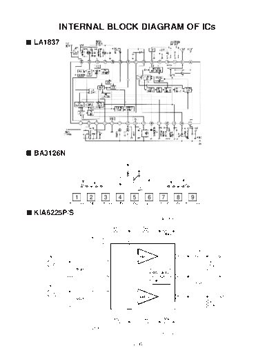
        INTERNAL BLOCK DIAGRAM OF ICs
I LA1837


I BA3126N


               1    2    3     4      5         6       7      8     9
            REC SW GND P/B SW CONT   GND        VCC   P/B SW   GND REC SW

I KIA6225P/S


                                     - 2-30 -
I KIA7805 P/PI ~ KIA7815 P/PI


I BU1923(FOR RDS/RBDS)


                            - 2-31 -
I BU2090F
Block diagram


                               Vss 1           Control circuit        16 VDD

                              DATA 2                                  15 Q11
                                             12-bit shift register
                             CLOCK 3                                  14 Q10
                                                    Latch
                                Q0 4                                  13 Q9
                                                 Output buffer
                                                 (open drain)
                                Q1 5                                  12 Q8

                                Q2 6                                  11 Q7

                                Q3 7                                  10 Q6

                                Q4 8                                   9 Q5


PIN DESCRIPTION

                  Pin No.
                                                    Pin name                        Function
 BU2090/F/FS       BU2092/F      BU2092/FV
       1                1              1               Vss           GND
       2                2              2             DATA            Serial data input
       3                3              3            CLOCK            Data shift clock input
       -                4              4              LCK            Data latch clock input
       4                5              5               Q0            parallel data output
       5                6              6               Q1            parallel data output
       6                7              7               Q2            parallel data output
       7                8              8               Q3            parallel data output
       8                9              9               Q4            parallel data output
       9                10             10              Q5            parallel data output
       10               11             11              Q6            parallel data output
       -                -              12             N.C.           Not connected
       -                -              13             N.C.           Not connected
       11               12             14              Q7            parallel data output
       12               13             15              Q8            parallel data output
       13               14             16              Q9            parallel data output
       14               15             17             Q10            parallel data output
       15               16             18             Q11            parallel data output
       -                17             19              OE            Output Enable
       16               18             20              VDD           Power supply


                                                - 2-32 -
I TDA7265

                                                                           +VS


                                                                                                    1000
◦ Jabse Service Manual Search 2026 ◦ Jabse Pravopis ◦ onTap.bg ◦ Other service manual resources online : Fixya ◦ eServiceinfo