Service Manuals, User Guides, Schematic Diagrams or docs for : LG Audio FFH-286AX IC

<< Back | Home

Most service manuals and schematics are PDF files, so You will need Adobre Acrobat Reader to view : Acrobat Download Some of the files are DjVu format. Readers and resources available here : DjVu Resources
For the compressed files, most common are zip and rar. Please, extract files with Your favorite compression software ( WinZip, WinRAR ... ) before viewing. If a document has multiple parts, You should download all, before extracting.
Good luck. Repair on Your own risk. Make sure You know what You are doing.


Image preview - the first page of the document
IC


>> Download IC documenatation <<

Text preview - extract from the document
                INTERNAL BLOCK DIAGRAM OF ICs
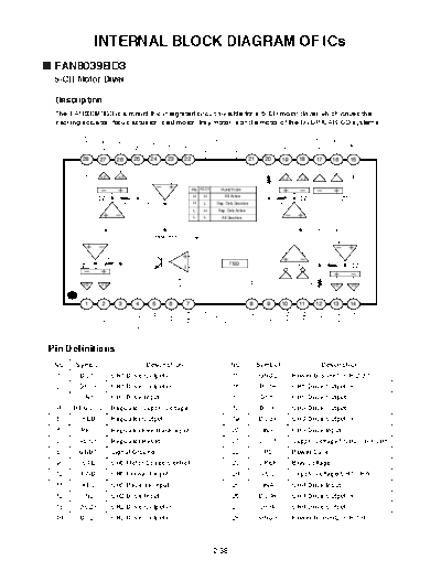
 FAN8039BD3
 5-CH Motor Diver

 Description
 The FAN8039BD3 is a monolithic integrated circuit suitable for a 5-CH motor driver which drives the
 tracking actuator, focus actuator, sled motor, tray motor, spindle motor of the DVDP/CAR-CD systems.


                                                                                                                          DO 3 +


                                                                                                                                                                                     GND2
                                                                                                                                                                    DO 5+
         GND3


                                                                                                                                                         DO 5-
                                                                                                     VCC1
                            DO 4+


                                                                                                                                       DO 3-
                                                      VREF
                  DO4-


                                                                                FIN

                                               VCC


                                                                                                                  IN3
                                                             PS
                                     IN4

                                                                               (GND)

         28      27        26        25        24     23     22                                      21           20       19           18               17         16               15


                    2           2                                                                           10K                2               2

                                                                    PS RESX       FUNCTION
                Level                                               H   H           All Active                                         Level                                 Level
                Shift                                                                                                                  Shift                                 Shift
                               10K                                  H   L       Reg. Only Deactive                       10K
                                                                    L   H       Reg. Only Active
                                                                    L   L          All Deactive


                                                 Regulator

                                                                        2.5V

                    10K
                                                                                                                                                                  10K
        Level                                                                          TSD                                           COMP                                            Level
        Shift                                                                                                                                                                        Shift


           2         2                                                                                                                             10K                   2                  2


          1       2          3       4          5      6      7                                      8             9      10            11               12         13               14


                                                                                                                                                                        DO 2+
                                                                                                                               FWD
                  DO1+


                                                             RESX


                                                                                                                                                                                      DO 2-
                                                                                                     GND1
                                                      REO
                                                REB


                                                                                                                                            REV
                                     REGVCC
         DO1-


                            IN1


                                                                                                                   CTL


                                                                                FIN                                                                        IN2
                                                                               (GND)


Pin Definitions
 NO    Symbol                                 Description                               NO                  Symbol                                               Description
 1      DO1-              CH1 Drive Output (-)                                           15                 GND2                     Power Ground1 (CH 2,3,5)
 2      DO1+              CH1 Drive Output (+)                                           16                 DO5+                     CH5 Drive Output (+)
 3       IN1              CH1 Drive Input                                                17                  DO5-                    CH5 Drive Output(-)
 4    REGVCC              Regulator Supply Voltage                                       18                 DO3-                     CH3 Drive Output(-)
 5      REB               Regulator Output                                               19                 DO3+                     CH3 Drive Output (+)
 6      REO               Regulator Feedback Input                                       20                  IN3                     CH3 Drive Input
 7      RESX              Regulator Reset                                                21                 VCC1                     Supply Voltage1(CH2,CH3,CH5)
 8      GND1              Signal Ground                                                  22                   PS                     Power Save
 9       CTL              CH5 Motor Speed Control                                        23                 VREF                     Bias Voltage
 10     FWD               CH5 Forward Input                                              24                  VCC                     Supply Voltage(CH1,CH4)
 11     REV               CH5 Reverse Input                                              25                  IN4                     CH4 Drive Input
 12      IN2              CH2 Drive Input                                                26                 DO4+                     CH4 Drive Output (+)
 13     DO2+              CH2 Drive Output (+)                                           27                  DO4-                    CH4 Drive Output (-)
 14     DO2-              CH2 Drive Output (-)                                           28                 GND3                     Power Ground2 (CH 1,4)


                                                                            - 2-38 -
 KA78R33
 Low Dropout Voltage Regulator

 Description
 The KA78R33 is a low-dropout voltage regulator suitable for various electronic equipments. It provides
 constant voltage power source with TO-220 4 lead full mold package. Dropout voltage of KA78R33 is
 below 0.5V in full rated current(1A). This regulator has various function such as peak current protection,
 thermal shut down, overvoltage protection and output disable function.

 Internal Block Diagram

                                                                                Q1
                Vin   1                                                                   2   Vo


                                                                OVERVOLTAGE
                                        THERMAL SHUTDOWN        PROTECTION


                                        BANDGAP REFERENCE       -
                                                                +
                                                                                     R1


                                                              SOA PROTECTION
                                 HIGH / LOW       OUTPUT
                                 4                ON / OFF
                          Vdis                -
                                              +
                                                                                     R2
                                                                    - CIRCUIT
                                                               SHORTCIRCUIT
                                 1.4V
                                                               PROTECTION


                                                                     3
                                                                    GND


 LC72131
 AM/FM PLL Frequency Synthesizer


                                                             - 2-39 -
 Block Diagram


             XIN                               REFERENCE                                PHASE DETECTOR   PD
                                               DIVIDER                                  CHARGE PUMP
           XOUT

                                                                                                         AIN
                                 1             SWALLOW COUNTER                          UNLOCK
            FMIN                                                                                         AOUT
                                     2           1/16. 1/17 4bits                       DETECTOR


            AMIN                                12bits PROGRAMMABLE
                                                        DIVIDER


             CE


              DI           CCB                  DATA SHIFT REGISTER                        UNIVERSAL     IFIN
                           I/F                        LATCH                                COUNTER

             CL


             D0

                           POWER
            VDD              ON
                           RESET

            VSS


                                         B01   B02   B03   B04               I01           I02


 LA1837
 Single-Chip Home stereo IC with Electronic Tuning Support
 The LA1837 is a single-chip AM/FM IF and MPX IC that supports electronic tuning and was developed for
 use in home stereo systems. It is optimal for use in automatic station selection systems that use the SD and
 IF counting techniques.

 Block Diagram
                   FM SD
                   ADJ


                                                                       3 rd 5 th
                                                                       DECODER
                                                                      ANTI-BIRDIE
                                                                                   FM


                                                           - 2-40 -
 KIA 78R12 PI
 4 TERMINAL LOW DROP VOLTAGE REGULATOR
 The KIA78RXX Series are Low Drop Voltage Regulator suitable for various electronic equipments. It
 provides constant voltage power source with TO-220 4 termainal lead full molded PKG. The Regulator has
 multi function such as over current protection, overheat protection and ON/OFF control.


                                              - 2-41 -
 Block Diagram


 KIA7805AP/API
 THREE TERMINAL POSITIVE VOLTAGE REGULATORS 5V, 6V, 8V, 9V, 10V, 12, 15V, 18V, 24V.

 EQUIVALENT CIRCUIT


                                        - 2-42 -
 BA3126N
 2-channel head switch for radio cassette recorders


                                     - 2-43 -
 BU2090F
 12-bit, Serial IN, Parallel OUT driver

 Block diagram


                              Vss 1             Control circuit         16 VDD

                         DATA 2                                         15 Q11
                                              12-bit shift register
                        CLOCK 3                                         14 Q10
                                                     Latch
                              Q0 4                                      13 Q9
                                                  Output buffer
                                                  (open drain)
                              Q1 5                                      12 Q8

                              Q2 6                                      11 Q7

                              Q3 7                                      10 Q6

                              Q4 8                                      9 Q5


 PIN DESCRIPTION

                   Pin No.
                                                             Pin name                     Function
   BU2090/F/FS      BU2092/F          BU2092/FV
         1               1                1                   Vss          GND
         2               2                2                  DATA          Serial data input
         3               3                3                  CLOCK         Data shift clock input
          -              4                4                   LCK          Data latch clock input
         4               5                5                       Q0       parallel data output
         5               6                6                       Q1       parallel data output
         6               7                7                       Q2       parallel data output
         7               8                8                       Q3       parallel data output
         8               9                9                       Q4       parallel data output
         9               10              10                       Q5       parallel data output
         10              11              11                       Q6       parallel data output
          -              -               12                   N.C.         Not connected
          -              -               13                   N.C.         Not connected
         11              12              14                       Q7       parallel data output
         12              13              15                       Q8       parallel data output
         13              14              16                       Q9       parallel data output
         14              15              17                   Q10          parallel data output
         15              16              18                   Q11          parallel data output
          -              17              19                       OE       Output Enable
         16              18              20                   VDD          Power supply


                                                - 2-44 -


◦ Jabse Service Manual Search 2024 ◦ Jabse PravopisonTap.bg ◦ Other service manual resources online : FixyaeServiceinfo