Service Manuals, User Guides, Schematic Diagrams or docs for : LG Audio cd321ax CD321IC

<< Back | Home

Most service manuals and schematics are PDF files, so You will need Adobre Acrobat Reader to view : Acrobat Download Some of the files are DjVu format. Readers and resources available here : DjVu Resources
For the compressed files, most common are zip and rar. Please, extract files with Your favorite compression software ( WinZip, WinRAR ... ) before viewing. If a document has multiple parts, You should download all, before extracting.
Good luck. Repair on Your own risk. Make sure You know what You are doing.


Image preview - the first page of the document
CD321IC


>> Download CD321IC documenatation <<

Text preview - extract from the document
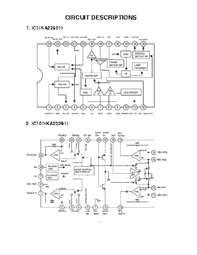
                                           CIRCUIT DESCRIPTIONS
1. IC1(KA22901)
                 AM RF IN          RF Vcc              FM OSC AM OSC                                          MPX IN        PH1                      PH1       OSC L-CH OUT
                         FM RF OUT                                                              DET OUT                                                                    R-CH OUT

                    24       23            22              21              20                       19          18          17                       16        15     14       13


                                                                                                                                                               OSC     STEREO
                                                                                                    AF                                                                 DETECTOR
                                                                                                              BUFFER
                                                                                                                              PHASE
                                                                                                                              DETECTOR                                 LAMP
                                AM F/E                                                                                                                                 TRUGGER

                                                                                                                                                               FF
                                                                                AM/FM DET


                                    FM F/E

                                                                                                              AM             FM
                                                                            AGC                                                                                LED DRIVER
                                                                                                              IF             IF


                    1           2           3              4               5                        6           7            8                        9        10     11       12
                 FM RF IN    GND          FM MIX       AM MIX              AGC                      Vcc        AM IF        FM IF                    GND TUNING LED    ST LED QUAD DET


2. IC101(KA22291)
                                                                                                           MUTE MUTE                                  REC
                                  PB NF(2)             PB IN(2)             R/P SW                         SW   IN                      ALC           OUT(2)

                                     23            22              21                           8              20      19                  18             15
                                                                                                                                                                       100K
                                                                                                                                 ALC TIME CONSTANT
                                                B-IN


                                                               A-AN


                                                                                R/P SW


                         100K


                                                                                                                                                                              IN PUT
                                     N.F                                                                                                                                               14   REC NF(2)
PB OUT(2)   24              PRE                                                                                                                                        PRE
                                                                                                                                                                              N.F
                                                                                                                                                                                       13   REC IN(2)
                                     INPUT
                                     REC.BLAS
      Vcc           RECORD
            16
                    I.FER                                   MODE CONTROL
                                                            /BLAS CIRCULT                                                                                            ALC
                                     PB.BIAS
                   PLAYBACK                                                                                                                                          DET
      Vcc   17
                   I.REF


REC GND     9
                                                                                                                                                                                       12   REC IN(1)
                                     INPUT
                                                                                A/B SELECT SW


                                                                                                                                                                              IN PUT
                                                                                                                                                                       PRE
PB OUT(1)   1               PRE
                                     N.F
                                                                                                                                                                              N.F
                                                                                                                                                                                       11   REC NF(1)
                                                                A-AN


                      100K                                                                                                                                             100K
                                                B-IN


                                      2                3               4                        5         7            6                                  10
                                  PB NF(1)             PB IN(1)                      A/B                  PB         MUTE                              REC
                                                                                     SW                   GND        IN(1)                             OUT(1)


                                                                                                              - 11 -
3. IC300(LA4227)
                   VCC           OUT 1       BS 1                               PWR GND (TAB)                                                  NF 1            IN 1          PRE GND

                   12             11             10                                                                                             9                8                      7


                                                                              Rf 1

                                                                                                                                     Rnf 1          62
                                                                           20k
                                                                                                        _
                                                                                        Ch1
                                                                                                        +

                                                 THERMAL
                                                 SHUT DOWN
                                                 PROTECTION
                           STANDBY                                                                                                                                          BIAS
                             SW                                                                                                                                             CIRCULT


                                                                                                        +
                                                                                        Ch2
                                                                                                        _

                                                                        20k
                                                                                                                                     Rnf 2          62
                                                                              Rf 2


                    1              2             3                                                                                              4                5                      6

                 STANDBY         OUT 2      BS 2                                PWR GND (TAB)                                                  NF 2            IN 2        DC (FILTER)


4. IC501(KB9223)
                                                                                                                  MDATA
                                                                      TRCNT


                                                                                                RESET
                                                            WDCH


                                                                                        ISTAT
                                                                                LOCK


                                                                                                                                                                                 FRSH
                                                                                                                                 ATSC
                                                                                                                          MCK


                                                                                                                                                                     FGD
                                                                                                            MLT


                                                                                                                                         TZC
                                           FE1

                                                      TE1


                                                                                                                                                         FE2
                                                                                                                                                               FLB


                                           59         54    22        30        29      31      38 37 36                  35     51      52              58    26    28    FS3
                                                                                                                                                                           27    3


       RF- 73                                                                                                                                                                               60   FDFCT
                                                                                                                                                         Focus Phase
                        RF Amp                                                           Micom Data
                                                                                                                                                         Compensation                       47   FE-
       RFO 74                                                                          Interface Logic
                                                                                                                                                         & Offset cancel circuit
                                                                                                                                                                                            48   FEO
       PD1 65
                                                                                                                                                                                            57   TDFCT
       PD2 66       Focus Error Amp
                    FE-BIAS Adjustment
     FEBIAS 63                                                                                                                                                                              49   TE-
                                                                                                                                                         Tracking Phase                     50   TEO
         F 67                                                                                                                                            Compensation Block
                    Tracking Error Amp
                                                                                                                                                         & Jump Pulse GEN.                  53   TE2
         E 68       E/F Balance & Gain
                    Control                                                                                                                                                                 55   LPFT
         EI 79                                                        MICOM TO SERVO CONTROL
                                                                          AUTO SEQUENCER                                                                                                    62   TG2
        PD 69                                                                                                                                                                               61   TGU
                                         LDON
                        APC Amp
        LD 70                                                                                                                                                                               43   SLO
                                                                   ADJUSTMENT-FREE CONTROL                                                               Sled Servo Amplifier               44   SL-
        VR 71        Center Voltage Amp.                                                                                                                 & Sled Kick GEN.
                                                                                                                                                                                            42   SL+
       EQC 78           RF Level AGC                                                                                                                                                        46   SPDLO
       EQO 76               &                                 FS1~               TM1~           BAL1~             PS1~           GA1~                                                       45   SPDL-
                                                                                                                                                         Spindle Servo LPF
                        Equalizer                             FS4                TM6            BAL5              PS4            GA5
        IRF 75                                                                                                                                           (Double Speed)                     23   SMDP
                                                                                                                                                                                            24   SMON
       ASY 32
                        EFM                                                                                                                                                                 25   SMEF
       EFM 33           Comparator
                                                                                                                                                                                            6    FSET
        RFI 77
                                                                                                                                                         MIRROR DETECTION                   39   MIRROR
                                                                                                                                                         CIRCUIT                            1    MCP
       DCB   2                                                         Built-in Post Filter Amp(L&R)
                    Defect Detection
                                                                                                                                                          FOK DETECTION
                    CircuitT                                                                                                                                                                40   FOK
      DCC2   4                                                                                                                                            CIRCUIT

                          5                                  15 16 13 14 19 17 12 11                                             9      10
                          DCC1


                                                               GC1O
                                                                         GC1I
                                                                                 CH1O
                                                                                         CH1I
                                                                                                MUTEI
                                                                                                            RRC
                                                                                                                  CH2O
                                                                                                                          CH2I
                                                                                                                                 GC2I
                                                                                                                                        GC2O


                                                                                                   - 12 -
 PIN DESCRIPTION (continued)KB9223

PIN NO SYMBOL   DESCRIPTION
 1    MCP       Capacitor connection pin for mirror hold
 2    DCB       Capacitor connection pin for defect Bottom hold
 3    FRSH      Capacitor connection pin for time constant to generate focus search waveform
 4    DCC2      The input pin through capacitor of defect bottom hold output
 5    DCC1      The output pin of defect bottom hold
 6    FSET      The peak frequency setting pin for focus, tracking servo and cut off frequency of
                CLV LPF
 7    VDDA      Analog VCC for servo part
 8    VCCP      VCC for post filter
 9    GC2I      Amplifier negative input pin for gain and low pass filtering of DAC output CH2
 10   GC2O      Amplifier output pin for gain and low pass filtering of DAC output CH2
 11   CH2l      The input pin for post filter channel2
 12   CH2O      The output pin for post filter channel2
 13   CHIO      The output pin for post filter channel1
 14   CH1I      The input pin for post filter channel1
 15   GC1O      Amplifier output pin for gain and low pass filtering of DAC output CH1
 16   GC1I      Amplifier negative input pin for gain and low pass filtering of DAC output CH1
 17   RRC       The pin for noise reduction of post filter bias
 18   VSSP      VSS for post filter
 19   MUTEI     The input pin for post filter muting control
 20   ISET      The input pin for current setting of focus search, track jump and sled kick voltage
 21   VREG      The output pin of regulator
 22   WDCK      The clock input pin for auto sequence
 23   SMDP      The input pin of CLV control output pin SMDP of DSP
 24   SMON      The input pin for spindle servo ON through SMON of DSP
 25   SMEF      The input pin of provide for an external LPF time constant
 26   FLB       Capacitor connection pin to perform rising low bandwidth of focus loop
 27   FS3       The pin for high frequencygain change of focus loop with internal FS3 switch
 28   FGD       Reducing high frequency gain with capacitor between FS3 pin
 29   LOCK      Sled runaway prevention pin
 30   TRCNT     Track count output pin
 31   ISTAT     Internal status output pin
 32   ASY       The input pin for asymmetry control
 33   EFM       EFM comparator output pin
 34   VSSA      Analog VSS for servo part


                                                  - 13 -
PIN NO SYMBOL   DESCRIPTION
 35   MCK       MICOM clock input pin
 36   MDATA     MICOM data input pin
 37   MLT       MICOM data latch input pin
 38   RESET     Reset input pin
 39   MIRROR    The mirror output for test
 40   FOK       The output pin of focus OK comparator
 61   TGU       The capacitor connection pin for high frequency tracking gain switch
 62   TG2       The pin for high frequency gain change of tracking servo loop with internal TG2 switch
 63   FEBIAS    Focus error bias voltage control pin
 64   DVEE      The DVEE pin for logic circuit
 65   PD1       The negative input pin of RF l/V amplifierl(A+C signal)
 66   PD2       The negative input pin of RF I/V amplifier2(B+D signal)
 67   F         The negative input pin of F l/V amplifier (F signal)
 68   E         The negative input pin of E I/V amplifier (E signal)
 69   PD        The input pin for APC
 70   LD        The output pin for APC
 71   VR        The output pin of (AVEE+AVCC)/2 voltage
 72   VCC       VCC for RF part
 73   RF-       RF summing amplifier inverting input pin
 74   RFO       RF summing amplifier output pin
 75   IRF       The input pin for AGC
 76   EQO       The output pin for AGC
 77   RFI       The input pin for EFM comparison
 78   EQC       The capacitor connection pin for AGC
 79   El        Feedback input pin of E I/V amplifier for EF Balance control
 80   GND       GND for RF part


                                                  - 14 -
5. (IC502)KA9258BD
           28       27         26         25         24       23           22                  21     20          19         18     17       16   15


                                               10K                                                          10K


                                                                    TSD
                 LEVEL                                                                                                              LEVEL
                 SHIFT                                                                                                              SHIFT
                                      10K                                                                         10K


                                                          REGULATOR
                         10K                                                        MUTE                          10K
         LEVEL                                                                                                                       LEVEL
                                                                         10K

         SHIFT                                                                                                                       SHIFT

                                                                                   50K   50K


                                    10K                            10K                                      10K


             1       2         3          4          5        6                7               8       9          10         11     12       13   14


    PIN DESCRIPTION KA9258BD
Pin No. Symbol       I/O                             Description                         Pin No. Symbol                I/O                    Description
1      DO1-1             O         Drive Output                                          15         OPIN(-)             I         OPamp Input(-)
2      DO1-2             O         Drive Output                                          16         OPIN(+)             I         OPamp output(+)
3      DI1-1             I         Drive Input                                           17         DO3-1               O         Drive Output(-)
4      DI1-2             I         Drive Input                                           18         DO3-2               O         Drive Output(+)
5      REG                         Regulator                                             19         DI3-I               I         Drive Input
6      REO               O         Regulator Output                                      20         DI3-2               I         Drive Input
7      MUTE              I         Mute                                                  21         VCC1                -         Supply Voltage
8      GND1              -         Ground                                                22         VCC2                -         Supply voltage
9      DI2.1             I         Drive Input                                           23         VREF                I         2.5V Bias Voltage
10     DI2.2             I         Drive Input                                           24         DI4.1               I         Drive Input
11     DO2.1             O         Drive Output                                          25         DI4.2               I         Drive Input
12     DO2.2             O         Drive Output                                          26         DO4.1               O         Drive Output(+)
13     GND2              -         Ground                                                27         DO4.2               O         Drive Output(-)
14     OPOUT             O         OPamp Output                                          28         GND3                -         Ground


                                                                                     - 15 -
6. IC503(KA9286B)


                                                                         SBCK


                                                                                  SDAT
                                                     S0S1
                                                     26


                                                                         32


                                                                                   33
                                                  SUBCODE               SUBCODE                   SUBCODE-Q                   30   SQDT
                                                  SYNC                  OUTPUT                    REGISTER                    29   SQCK
                                                  DETECTOR


                EFM                               23BIT                   EFM
   EFMI    66   PHASE                             SHIFT                   DEMODULATOR
                DETECTOR                          REGISTER


                                                                                                              8BIT DATA BUS
 CNTVOL    5
                DIGITAL                                                   ADDRESS
  DPFIN    3    PLL                                                       GENERATOR
                                                  FRAME SYNC
 DPFOUT    4                                      DETECTOR
                                                  PROTECTOR
  DPDO     2
                                                  INSERTOR                      16K
  SMEF     72                                                                   SRAM
                 DIGITAL
  SMON     73
  SMDP     75
                 CLV
  SMSD     76
                 SERVO
  LOCK     70                                                                   ECC
                                                  X-TAL
   XOUT    9
                                                  TIMING
     XIN   8                                      GENERATOR                     INTERPOLATOR

                                                                                                                              11   LRCHO
                                                                                                                              12   ADATAO
           37
                                                                                                                              14   BCKO
  MDAT
   MCK     38    CPU                               TRACK
                 INTERFACE                         COUNTER                                                                    77   BCKI
   MLT     36                                                                      DIGITAL
                                                                                                                              67   ADATAI
                                                                                   FILTER                                          LRCHI
  TRCNT    69                                                                                                                 60
                                                                                   & DE-EMPH
  /ISTAT   68                                                                                                                 24   EMPH

                    MODE                           DIGITAL                        D/A                                         17   VREFL1
                    SELECTOR                       OUTPUT                         CONVERTER                                   22   VREFH1
                 61

                          62

                                  63

                                          65


                                                                                      19


                                                                                                20
                                                      7
                XTALSEL

                          TEST0
                                  CDROM

                                          TEST1


                                                      DATX


                                                                                      RCHOUT


                                                                                               LCHOUT


                                                               - 16 -
  PIN DESCRIPTION KS9286B

PIN NO   SYMBOL   I/O                                DESCRIPTION
  1      AVDD1     -    Analog VCC1
  2      DPDO     O     Charge pump output for Digital PLL
  3      DPFIN     I    Filter input for Digital PLL
  4      DPFOUT   O     Filter output for Digital PLL
  5      CNTVOL    I    VCO control voltage for Digital PLL
  6      AVSS1     -    Analog Ground 1
  7       DATX    O     Digital Audio output data
  8       XIN      I    X tal oscillator input
  9       XOUT    O     X tal oscillator Output
 10      WDCHO    O     Word clock output of 48bit/Slot (88.2KHz)
 11      LRCHO    O     Channel clock output of 48 bit/Slot (44.1 KHz),88.2KHz when ESP ON
 12      ADATAO   O     Serial audio data output of 48 bit/Slot(MSB first), double speed output
                        when ESP ON
 13       Dvss1    -    Digital Ground1
 14       BCKO    O     Audio data bit clock output of 48 bit/Slot (2.1168MHz),4.2336MHz when
                        ESP ON
 15       C2PO    O     C2 Pointer for output audio data
 16      VREFL2    I    Input terminal2 of reference voltage L (Floating)
 17      VREFL1    I    Input terminal1 of reference voltage L (GND connection)
 18      AVDD2     -    Analog VCC2
 19      RCHOUT   O     Right-Channel audio output through D/A converter
 20      LCHOUT   O     Left-Channel audio output through D/A converter
 21      AVSS2     -    Analog ground2
 22      VREFH1    I    Input terminal1 of reference voltage H (VDD connection)
 23      VREFH2    I    Input terminal2 of reference voltage H (Floating)
 24      EMPH     O     Emphasis/Non-Emphasis output, H: Emphasis ON, L: Emphasis OFF
 25       LKFS    O     The Lock Status output of frame sync
 26       S0S1    O     Output of subcode sync signal(SO+S1)
 27      RESET     I    System reset at L
 28       /ESP     I    ESP function ON/OFF control ( L : ESP function ON, H : ESP function
                        OFF)
 29       SQCK     I    Clock for output Subcode-Q data
 30       SQDT    O     Serial output of Subcode-Q data
 31      SQOK     O     The CRC (Cycle Redundancy Check) check rssult signal output of
                        Subcode-Q


                                                 - 17 -
PIN NO   SYMBOL    I/O                           DESCRIPTION
 32       SBCK      I    Clock for output subcode data
 33       SDAT     O     Subcode serial dsta output
 34      DVDD1      -    Digital VDD1
 35       MUTE      I    Mute control input ( H : Mute ON)
 36       MLT       I    Latch Signal Input from Micom (Schmit Trigger)
 37       MDAT      I    Serial data input from Micom (Schmit Trigger)
 38       MCK       I    Serial clock input from Micom (Schmit Trigger)
 39       DB8      I/O   SRAM data I/O port 8 (MSB)
 40       DB7      I/O   SRAM data I/O port 7
 41       DB6      I/O   SRAM data I/O port 6
 42       DBS      I/O   SRAM data I/O port 5
 43       DB4      I/O   SRAM data I/O port 4
 44       DB3      I/O   SRAM data I/O port 3
 45       DB2      I/O   SRAM data I/O port 2
 46       DB1      I/O   SRAM data I/O port 4 (LSB)
 47       C1F1     I/O   Monitoring output for C1 error correction (RA1)
 48       C1F2     I/O   Monitoring output for C1 error correction (RA2)
 49       C2F1     I/O   Monitoring output for C2 error correction (RA3)
 50       C2F2     I/O   Monitoring output for C2 error correction (RA4)
 51       C2FL     I/O   C2 decoder flag (RA5, H : When the processing C2 code is impossible
                         correction status)
 52       /PBCK    I/O   Output of VCO/2 (4.3218MHz) (RA6)
 53      DVSS2     I/O   Digital ground 2
 54       FSDW     I/O   Window or unprotected frame sync (RA7)
 55      ULKFS     I/O   Frame sync protection state (RA8)
 56        /JIT    I/O   Display of either RAM overflow or under flow for   4 frame jitter margin
                         (RA9)
 57       C4M      I/O   Only monitoring signal (4.2336MHz) (RA10)
 58       C16M     I/O   16.9344MHz signal output(RA11)
 59       /WE      I/O   Terminal for test
 60        /CS     I/O   Tsrminal for test
 61      XTALSEL    I    Mode Selectiona1(H: 33.8688MHz, L: 16.9344MHz)
 62       TEST0     I    TEST input terminal (GND connection)
 63      CDROM      I    Mode Selection2 (H: CD-ROM, L: CDP)
 64       SRAM      I    TEST input tsrminal (GND connection)
 65       TEST1     I    TEST input terminal (GND connection)


                                             - 18 -
PIN NO SYMBOL                I/O                                  DESCRIPTION
 66           EFMI               I     EFM signal input
 67          ADATAI              I     Serial audio data input of 48 bit/Slot (MSB first)
 68          /ISTAT          O         The internal status output
 69          TRCNT               I     Tracking counter input signal
 70           LOCK           O         Output signal of LKFS condition sampled PBFR/16 (if LKFS is H , LOCK
                                       is H , if LKFS is sampled L at least 8 timss by PSFR/16, LOCK is L .)
 71           PBFR           O         Write frame clock (LDck: 7.35KHz)
 72          SMEF            O         LPF time constant control of the spindle servo error signal
 73          SMON            O         ON/OFF control signal for spiNdle servo
 74          DVDD2               -     Digital VDD2
 75          SMDP            O         Spindle Motor drive (Rough control in the SPEED mode, Phase control in
                                       the PHASE mode)
 76          SMSD            O         Spindle Motor drive (Velocity control in the PHASE mode)
 77           BCKI               I     Audio data bit clock input of 48 bit/slot (2.1168MHz)
 78          TESTV               I     TEST input terminal (GND connection)
 79          DSPEED              I     TEST input terminal (VDD connection)
 80          LRCHI               I     Channel clock input of 48 bit/Slot (44.1 KHz)


7. IC601(KS57C0408B)
                                                                           BASIC      WATCH
                                                                           TIMER      TIMER
                         INT0, INT1,
                         INT2, INT4       RESET         Xin     Xout

                    8-BIT                                                                                   P0.0 / SCK
                   TIMER/                                                                                   P0.1 / SO
                 COUNTER 0                                                                    I/O PORT 0
                                        INTERRUPT                         INSTRUCTION                       P0.2 / SI
                                         CONTROL          CLOCK             REGISTER                        P0.3 / BTCO
                                          BLOCK
                    8-BIT
                   TIMER/                                                                      SERIAL
                 COUNTER 1                                                  PROGRAM              I/O
                                                                            COUNTER                        P1.0 / INT0
                                         INTERNAL
                                       INTERRUPTS                                                          P1.1 / INT1
                                                                                               INPUT       P1.2 / INT2
P4.0-P4.3            I/O PORT4
                                                                                               PORT 1      P1.3 / INT4
                                         INSTRUCTION DECODER                PROGRAM
P5.0-P5.3            I/O PORT5                                            STATUS WORD
                                                                                                           P2.0 / TCLO0
                                               ARITHMETIC                                     I/O PORT 2   P2.1 / TCLO1
                                                   AND                       STACK                         P2.2 / CLO
P6.0-P6.3/
                     I/O PORT6                 LOGIC UNIT                   POINTER                        P2.3 / BUZ
KS0-KS3

P7.0-P7.3/                                                                                    I/O PORT 3   P3.0 / TCL0
                     I/O PORT7
 KS4-KS7                                                                                                   P3.1 / TCL1
                                                                                                           P3.2
                                                                                                           P3.3

P8.0-P8.3            I/O PORT8                                         PROGRAM MEMORY
                                                                       4 KBYTE:KS57C0404
                                                                       8 KBYTE:KS57C0408


                                                              - 19 -
 PIN DESCRIPTIONS (KS57C0408B)

Pin Name    Pin Type                           Description                                  Number Share Pin
P0.0          I/O      4-bit I/O port.                                                      12 (28)     SCK
P0.1                   1-bit or 4-bit read/write and test is possible.                      11(27)       SO
P0.2                   Individual pins are software configurable as input or output.        10(26)       SI
P0.3                   4-bit pull-up resistors are software assignable; pull-up              9(25)      BTCO
                       resistors are automatically disabled for output pins.
P1.0           I       4-bit input port.                                                     4 (20)     INT0
P1.1                   1 -bit and 4-bit read and test is possible.                           3 (19)     INT1
P1.2                   3-bit pull-up resistors are assignable by software to                 2 (18)     INT2
P1.3                   pins P1.0, P1.1, and P1.2                                             1(17)      INT4
P2.0          I/O      Same as port 0.                                                       8 (24)    TCLO0
P2.1                                                                                         7 (23)    TCLO1
P2.2                                                                                         6 (22)     CLO
P2.3                                                                                         5 (21)     BUZ
P3.0          I/O      Same as port 0.                                                      20 (38)     TCL0
P3.1                                                                                        19 (37)     TCL1
P3.2                                                                                        18 (36)
P3.3                                                                                        17 (35)
P4.0-P4.3     I/O      4-bit I/O ports.                                                      26-23
                       N-channel open-drain output up to 9 volts.                           (44-41 )
P5.0-P5.3              1 -bit rind 4-bit read/write and test is possible.                    30-27
                       Port 4 and 5 can be paired to support 8-bit data transfer.            (4-1)
                       8-bit unit pull-up resistors are assignable by mask option.
P6.0-P6.3     I/O      4-bit I/O ports.                                                      37-34     KS0-KS3
                       1 -bit or 4-bit read/write and test is possible.                     (11-8)
P7.0-P7.3              Port 6 pins are individually software configurable as                 41-38 KS4-457
                       input or output                                                      (15-12)
                       4-bit pull-up resistors are software assignable; pull-up
                       resistors are automatically disabled for output pins(port 6 only).
                       Ports 6 and 7 can be paired to enable 8-bit data transfer.
P8.0-P8.3     I/O      4-bit I/O ports.                                                      16-13
                       1 -bit and 4-bit read/write and test is possible.                    (32-29)
                       Pins are individually software configurable as input or output.
                       4-bit pull-down resistors are software assignable;pull-down
                       resistors are automatically disabled for output pins


                                                      - 20 -
 PIN DESCRIPTIONS (KS57C0408B)

Pin Name     Pin Type                        Description                                 Number Share Pin
SCK            I/O      Serial I/O interface clock signal                                12 (28)     P0.0
SO             I/O      Serial data output                                               11(27)      P0.1
SI             I/O      Serial dots input                                                10 (26)     P0.2
BTCO           I/O      Basic timer clock output (2 Hz, 16 Hz,64 Hz, or 256              9 (25)      P0.3
                        Hz at 4.19 MHz)
INT0, INT1      I       External interrupts. The triggering edge for INTO and              4,3    P1.0, P1.1
                        INT1 is selectable. INT0 is synchronized to system clock.        (20, 19)
INT2            I       Quasi-interrupt with detection of rising edges                   2 (18)      P .2
INT4            I       External interrupt with detection of rising and falling edges.   1 (17)      P1.3
TCLO0          I/O      Timer/counter 0 clock output                                     8 (24)      P2.0
TCLO1          I/O      Timer/counter 1 clock output                                     7 (23)      P2.1
CLO            I/O      Clock Output                                                     6 (22)      P2.2
BUZ            I/O      2 kHz,4 kHz,8 kHz, or 16 kHzfrequency output at 4. 9             5 (21)      P2.3
                        MHz for buzzer sound
TCL0           I/O      External clock input for timer/counter 0                         20 (38)     P3.0
TCLI           I/O      External clock input for timer/counter 1                         19 (37)     P3.1
KS0-KS3        I/O      Quasi-interrupt inputs with falling edge detection               37-34     P6.0-P6.3
                                                                                         (11-8)
KS4-KS7                                                                                  41-38     P7.0-P7.3
                                                                                         (5-12)
VDD             -       Power supply                                                     21 (39)
VSS             -       Ground                                                           42 (16)
RESET           I       Reset signal                                                     31 (5)
Xin, Xout       -       Crystal, ceramic, or RC oscillator signal for system clock        33,32
                        (For external clock input, use Xin and input Xin s                 (7,6)
                        reverse phase to Xout)
TEST            -       Test signal input (must be connected to VSS)                     22 (40)
NC              -       No connection (must be connected to VSS)                         (33,34)


                                                   - 21 -
MAJOR WAVEFORM

             TRACKING ERROR(REW)                                 TRACKING ERROR(FWD)

      V1=0.00V      TRIG 1=1.0V    T=0.00ms                V1=0.00V     TRIG 2=1.0V    T=0.00ms
      V2=0.00V                       SAVE                  V2=0.00V     SREF 2 A

1                                                   1


2                                                   2
                               DLY>=0.85ms                                         DLY>=0.85ms
      1V       1V      PEAKDET 1ms   1ms                  1V       1V      PEAKDET 1ms   1ms


◦ Jabse Service Manual Search 2024 ◦ Jabse PravopisonTap.bg ◦ Other service manual resources online : FixyaeServiceinfo