Service Manuals, User Guides, Schematic Diagrams or docs for : LG Car Audio tch-300 TCH-30~3

<< Back | Home

Most service manuals and schematics are PDF files, so You will need Adobre Acrobat Reader to view : Acrobat Download Some of the files are DjVu format. Readers and resources available here : DjVu Resources
For the compressed files, most common are zip and rar. Please, extract files with Your favorite compression software ( WinZip, WinRAR ... ) before viewing. If a document has multiple parts, You should download all, before extracting.
Good luck. Repair on Your own risk. Make sure You know what You are doing.


Image preview - the first page of the document
TCH-30~3


>> Download TCH-30~3 documenatation <<

Text preview - extract from the document
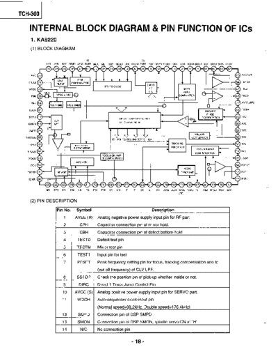
TCH-3001

     INTERNAL BLOCK DIAGRAM & PIN FUNCTION OF ICs
      1. KA9220
      (1) BLOCK DIAGRAM


                                               6)                                           (S)
             SET   APDI   BPF   EFMO   AASC   DVEE   MCK     MLT MDAT RESET DIRC TRCNT AVEE TEST1 ISTAT PFSET CBH           CPH   TESTH SSTOP   SLEI   SLEO   SLEN   TEST2


      FVC                                                                                                                                                                    AVCC    (S)


    VREGI                                                                                                                                                                    TDF CT


    VREG                                                                                                                                                                     TKEI


      F8M                                                                                                                                                                    TKEO


       N/C                                                                                                                                                                   AVCC    (RF)


     LOCK                                                                                                                                                                    TGSW


    SMPD                                                                                                                                                                     RTG
                                                                          MICOM TO SERVO CONTROL
                                                                          AUTO SEQUENCER
    SMON                                                                                                                                                                     ATS


    SMEF                                                                                                                                                                     TZC


  DVCC(S)                                                                                                                                                                    TE2


     SPDI                                                                                                                                                                    TEl


   SPDLO                                                                                                                                                                     N/C


    WDCH                                                                                                                                                                     FSCH


      FOK                                                                                                                                                                    FDFCT


   TESTD                                                                                                                                                                     FCE


    LDON                                                                                                                                                                     FSEO


             RFI   RF0    RF-    P/N    LD    PD     PDl     PD2   CV   N/C    F      E     EO     El     RV   DCC2 DCCl   AVEE FBIAS FE1       FE2    HFGD   FSW     LFR
                                                                                                                           (RF)


     (2) PIN DESCRIPTION

                    IPin No. 1 Symbol                1                                                  Description

                           1           AVEE (R)            Analog negative         power supply input pin for RF part

                           2             CPH               Capacitor    connection        pin of mirror hold.

                    I      3     1       CBH         1 Capacitor        connection        pin of defect bottom-hold

                    I      4           TESTD         1 Defect test pin

                    I      5     /     TESTM         / Mirror test pin

                    I      6     1 TEST1             / Input pin for test
                           7            PFSET              Peak frequency      setting pin for focus, tracking compensation                        and fc

                                 I                   I (cut off frequency)          of CLV LPF.

                    I      8     1 SSTOP             I Check the position pin of pick-up whether inside or not.
                           9     /      DIRC         I Direct 1 Track Jump Control Pin
                          IO     I AVCC (s) I Analog positive power supply input pin for SERVO part.

                          11            WDCH               Auto-sequencer      clock-input         pin

                                 I                   I (Normal speed=88.2kHz,                    Double speed=1 76.4kHz)

                          FrSMPD                     1 C onnection        pin of DSP SMPD

                          13     1      SMON         1 C onnection        pin of DSP SMON, spindle servo ON at "H"

                          I4 I           N/C         I No connection          pin


                                                                                    -18-
                                                                                                                     ITCH-300
    Pin No. 1 Svmbol      1                                         Description

      15         TGSW         Providing time constant to change the high frequency             tracking gain

      16          RTG         Capacitor    connection       pin switch the tracking gain of high frequency
-     17          LFR         Capacitor connection          pin to perform rising low bandwidth    of focus

                              servo loop

      18          FSW         High frequency     gain of focus servo loop can be changed by FS3
                    .         switch ON or OFF

      19         HFGD         Reducing high frequency          gain with capacitor connected      between

                              pin 18 and pin 19.

      20         FSCH     1 Time constant external pin to qenerate focus search waveform
                                                          _
      21   1 VREGI        1 External reaulator voltage input pin for VCO
      22   1      ISET    I Determina the peak value of focus            search, track jump and SLED kick

      23   I    VREG      I 3.5~ Reaulator output pin
      24   I     FVC      I Pin connected       external     resistor to adjust free runninqL frequency     of VCO

      25   I    SMEF      I   Providinq an external         LPF time constant of CLV SERVO loop

      26   I     BPF      I Providinq time constant for Loop filter of VCO
      27   1     MCK      1 Clock input pin from micom
      28   )     MLT      I Latch input pin from micom
      29   I    MDAT      1 Data input pin from micom
      30   I RESET        1 Reset input pin from micom, reset at "~11
      31   I    LOCK      I Pin for operation of the sied runaway prevention            function at "L"

      32   I TRCNT        I Track count output pin
      33   I    ISTAT     I Internal status output pin
      34       AVEE (S)       Analog negative     power supply input pin for SERVO part

      35        APDI          Input pin of DSP phase comparison           output (PHAS)

      36         F8M          Output pin of analog VCO

           I              I Normal speed=8.64MHz,              Double speed=1 7.28MHz

      37   1 AASC         1 Auto-Asvmmetrv        control input pin

      38   1 EFMO         1 EFM comoarator        outout pin

      39   )    SLEN      1 N on-inverting    input pin of SLED SERVO amplifier

      40   I    SLEO      1 Output pin of SLED SERVO amplifier

      41   1    SLEI      1 Inverting input pin of SLED SERVO amplifier
      42       TEST2          Test input pin to change speed mode

           I              I Normal speed= "H", Double speed= "L"
      43        SPDI          Inverting input pin of spindle servo amplifier

      44       SPDLO          Spindle servo amplifier output pin

      45   I     FCE      1 lnvertinq input pin of focus servo complifier.
      46   I    FSEO      I OutDut pin of focus servo amplifer
      47        TKEI          Non-inverting   input pin of tracking servo amplifier

      48   /    TKEO      / Output pin of tracking servo amplifier


                                                        I
                                                             19-
-   TCH-3001
               Pin No.        Symbol                                       Description

                     49         N/C        No connection

               I     50         ATS        Anti-shock   input pin

                                           Tracking Zero Crossing input pin

                                           Tracking Error Servo input pin

                                TEI        Output pin of trackina Error Amolifer
                     54   ( TDFCT        1 Capacitor Connection       pin for Defect Compensation     of tracking servo

                     55       DVCC(S)      Digital positive power supply input pin for servo part

                     56         FE2        Focus error servo input pin

                     57         FE1        Output pin of focus error Amplifer

                     58       FDFCT        Capacitor connection       pin for defect compensation    of focus servo

                     59         FOK        Output pin of Focus ok comparator.

                     60        LDON        Laser diode ON/OFF control pin

                     61          El        Feedback     input pin of E I-V amplifier

                     62         EO         Output pin of E I-V Amplifier

                     63        FBIAS       Bias pin of non-inverting     input of focus error amplifier

                     64       DVEE (S)     Digital negative   power supply input pin for servo part

                     65         RFI        Output Signal of RF summing amplifier is inputed through capacitor

                     66         RF0        Output pin of RF summing amplifier

                     67         RF-        inverting input pin of RF summing amplifier

                     68         RV         Output pin of (AVCC+AVEE)/2          Voltage

               r     69         CV         Bias input pin of Center Voltage buffer

               r70        1      LD      / Output pin of APC amplifier
               r-    71   /     PD       I Input pin ~~ APC amplifier
                                                      of

                     72       AVCC( R)     Analog positive power supply input pin for RF part

                     73         N/C        No connection

                     74         PD2        Inverting input pin of RF I-V AMP2
                     75         PDI        Inverting input pin of RF I-V AMP1

               I     76          F         Inverting input pin of FI-V AMP

                     77          E         Inverting input pin of E I-V AMP

                     78         P/N        Selecting    P-sub/N-sub    of Laser diode

                     79        DCC2        Defect bottom-hold       output is inputed through capacitor
                     80        DCCI        Output pin of defect bottom-hold


                                                                      - 20 -
                                                                      TCH-300
2. KS9282
(1) BLOCK DIAGRAM


                        SOS1     SBCK SDAT     SQEN SQCK


                                                               SQDT

                                                               SQOK


             EFMI

            APDO
                     28 bits
                     shift
                     register
                                                IT-        r


            VCOII


            DPDO

            DPFIN   Frame
                    sync
        DPFOUT      detector
                    protector
        CNTVOL      insertor

        DSPEED

            SMEF
            SMON
            SMPD
            SMSD     X'tal

            LOCK

              XIN

            XOUT

              MLT                  +   Digital Filter
                                       (8 ts1
            MDAT
             MCK


                      DATX        RCHOUT       LCHOUT


                          -21,
TCH-300

    (2) PIN CONFIGURATION


                           DPDO                                                                   SEL3
                           DPFIN                                                                  SEL2
                          DPFOUT                                                                  SELl
                          CNTVOL                                                                  /cs
                           AVSSl                                                                  /WE
                            DATX                                                                  C16M
                             XIN                                                                  C4M
                           XOUT                                                                   /JIT
                          WDCHI                                                                   ULKFS
                           LRCHl                                                                  FSDW
                          ADATAl                                                                  DVSS2
                           DVSSI                             KS9282                               /PBCK
                             BCK                                                                  C2FL
                           C2PO                                                                   C2F2
                            TIM2                                                                  C2Fl
                           /BCKl                                                                  ClF2
                           /BCK2                                                                  Cl Fl
                            BCK2                                                                  DBI
                           LRCH2                                                                  DB2
                          ADATA                                                                   DB3
                             N.C                                                                  DB4
                          WDCH2                                                                   DB5
                           EMPH                                                                   DB6


    (3) PIN DESCRIPTION
                                                                                                          -
            Pin No.        Symbol       I/O                                      Description

               1           AVDDI                  Analog Vcc 1

               2            DPDO    1 0       (   Charge pump output for master PLL

               3           DPFIN    I   '     I   Filter input for master PLL    '

               4          DPFOUT        0         Filter output for master PLL

               5          CNTVOL        I         VCO Control Voltage for master PLL

               6           AVSSI    I         I   Analog Ground 1

               7      I     DATX    1 0       1   Digital audio output

               8             XIN                  X-tal oscillator   input

               9           XOUT                   X-tal oscillator output

              10      )   WDCHI     (   0     (   Word clock of 48 bit/SLOT

                                                  (Normal speed=88.2kHz,      Double speed=1 76.4kHz)


                                                              - 22 -
                                                                                                     9   TCH-300


1 Pin No. 1   Symbol   1 I/O     1                                       Description

/   11   1     LRCH    1 0       (   Channelclock       of 48 bit/SLOT

                                     (Normal speed=44.1 kHz, Double speed=88.2kHz)

I   12   1    ADATA    1 0       1   S erial audio data output of 48 bit/SLOT (MSB first)

I   13        DVSSI    I         I   Digital Ground 1


I I4I BCK
                                     Audio data Bit clock for 48 bit/SLOT

                                     (Normal speed=2.1168kHz,        Double speed=4.2336kHz)

I   15         C2PO    1 0       )         ~~
                                     C2 pointer for output audio data

I   16   I    VREFL2   I     I   I   Input terminal 2 of reference voltage "L" (Floating)

I   17   1 VREFLI      )     I   (   Input terminal    1 of reference voltage "L" (GND connection)

I   18   1    AVDD2    )         1 Analog VCC2

I   19   I RCHOUT      I    0    I   Right-channel     audio output through D/A convertes

I   20        LCHOUT        0        Left-channel     audio output through D/A converter

I   21        AVSS2              I   Analog ground 2

I   22   )    VREFHI   I    I    I   Input terminal    1 of reference voltage "H" (VDD connection)

I   23   I    VREFH2   (    I    )   Input terminal 2 of reference voltage "H" (Floating)

I   24         EMPH    1 0       1   Emphasis/Non-Emphasis         output ("H": Emphasis)

    25         LKFS         0        The lock status output of frame sync

    26         SOS1         0        Output of subcode sync signal (SO+Sl)

    27        RESET         I        System reset at "L"

    28        SQEN          I        SQCK I/O Control ("L" : internalCK,        "H" : external CK)

    29        SQCK         I/O       Clock for output subcode-Q      data

    30        SQDT         0         Serial output of subcode-Q     data

    31        SQOK         0         The CRC Check result signal output of subcode-Q

    32        SBCK          I        Clock for output subcode-       data

    33        SDAT         0         Subcode Serial data output

    34        DVDDI                  Digital Vcc 1

    35        MUTE          I        Mute control Input ("H" : Mute ON)

    36         MLT          I        Latch signal input from Micom

    37        MDAT          I        Serial data input from Micom

    38         MCK          I        Serial clock input from Micom

    39         DB8         I/O       SRAM data I/O Port 8 (MSB)

    40         DB7         I/O       SRAM data I/O Port 7

    41         DB6         I/O       SRAM data I/O Port 6

    42         DB5         I/O       SRAM data I/O Port 5

    43         DB4         I/O       SRAM data I/O Port 4

    44         DB3         I/O       SRAM data I/O Port 3

    45         DB2         I/O       SRAM data I/O Port 2

    46         DBI         I/O       SRAM data I/O Port 1 (LSB)


                                                       - 23 -
TCH-300


          Pin No.       Symbol       I/O                                         Description
              47         Cl Fl       I/O       Monitoring    output for Cl error Correction         (RAI)
              48         ClF2        I/O       Monitoring    output for Cl error Correction         (RA2)
              49         C2Fl        I/O       Monitoring    output for C2 error Correction         (RA3)
              50         C2F2        I/O       Monitoring    output for C2 error Correction         (RA4)
              51         C2FL        I/O       C2 decoder flag (High: When the processing               C2 code is
                                               impossible    correction   state) (RA5)
                                                             VCO (Normal speed = 4.3218MHz
              52        /PBCK        I/O       output   of   -
                                                               2 Double speed = 8.6436MHz)                  (RA6)
              53        DVss2                  Digital Ground 2
              54        FSDW         I/O       Unprotected     frame Sync (RA7)
              55        ULKFS        I/O       Frame sync protection       state (RA8)
              56         /JIT        I/O       Display of either RAM overflow       or underflow for +4 frame Jitter margin
                                               (RA9)
              57         C4M         I/O       Only Monitoring     signal (Normal playback:         4.2336MHz)
                                               (RAIO)
              58    1    C16M    1 I/O     1 16.9344MHz        signal output (RAI 1)
              59         /WE         I/O       Terminal for test
              60         ICS         I/O       Terminal for test
              61         SELI         I        Mode Selection Terminal        1 (H: 33.8688MHz)
                                                                                (L: 16.9344MHz)
              62         SEL2         I        Mode Selection Terminal 2 (H: APLL)
                                                                                (L: DPLL)
              63         SEL3         I        Mode Selection Terminal 3 (H: CDROM)
                                                                                (L: CDP)
              64         SEL4         I        Mode Selection Terminal 4 (L: Internal SRAM)
              65         TEST         I        Test Terminal     (L: Normal operating      state)
              66         EFMI         I        EFM Signal input
              67        APDO         0         Charge Pump output for analog PLL
              68    1   /ISTAT   I   0     I   The internal status output
              69        TRCNT    I
                                      I        Tracking counter input signal
                                                                                       PBFR
              70         LOCK        0         Output signal of LKFS condition sampled -
                                                                                         16
                                               (If LKFS is "H", Lock is "H".                                                  --
          .                                                                                   PBFR
                                               If the LKFS is sampled "L" at least 8 times by -      Lock is `IL")
                                                                                                16 '
              71    I    PBFR    1 0       1   Write frame clock (Lock: 7.35kHz)
              72    I    SMEF    I   0     I   LPF time constant control of the spindle servo error signal
              73        SMON         0         ON/OFF control signal for spindle servo
              74        DVDD2                  Digital Vcc2
              75        SMPD         0         Spindle Motor drive (Rough control in the CLV-S mode
                                                                          Phase control in the CLV-P mode)
              76        SMSD         0          Spindle Motor drive (Velocity control in the CLV-P mode)
              77        VCOOl        0         VCO output signal (When the state is Lock by means of PBFR it is
                                               8.643MHz)
              78         VCOII        I        VCO input signal
              79        DSPEED        I        Double speed mode control (H: Normal speed)
                                                                                 (L: Double speed)
              80        APD02        0         Analog PLL charge pump output for Double speed mode


                                                                 - 24 -


◦ Jabse Service Manual Search 2024 ◦ Jabse PravopisonTap.bg ◦ Other service manual resources online : FixyaeServiceinfo