Service Manuals, User Guides, Schematic Diagrams or docs for : LG TV CT-25Q26ET 077A_TRO

<< Back | Home

Most service manuals and schematics are PDF files, so You will need Adobre Acrobat Reader to view : Acrobat Download Some of the files are DjVu format. Readers and resources available here : DjVu Resources
For the compressed files, most common are zip and rar. Please, extract files with Your favorite compression software ( WinZip, WinRAR ... ) before viewing. If a document has multiple parts, You should download all, before extracting.
Good luck. Repair on Your own risk. Make sure You know what You are doing.


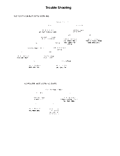
Image preview - the first page of the document
077A_TRO


>> Download 077A_TRO documenatation <<

Text preview - extract from the document
                                               Trouble Shooting


                                                                                                          3V


                                     Q05, IC851, IC802(3), IC856.                            pin 32 of IC01.

                                                                                      3.3V                           0V

                                                     ICP(V)01.
                                                                                IC01, FR403, FR413,            IC852(3), IC854(5), FR406,
                                                                                 D405, D406, IC301,               D408, D858, Q856.
                                                                                      ICP(V)01.


                                                                    ICP(V)01.
                                                     33V


F854, D861, R405.

                                                                                 (OPTION)


                    D850, L853, T402.                            Q401, Q402, T401.


                                                                     C804


                              pin4                                       F(P)801, SW(P)801, T1111,
                                                                            T801, R802, DB801.
                                                           18V


                T802, R809, D802.
                                    ICP(V)01.


             37~39   ICP(V)01.              12


 ICP(V)01.               CPT PCB ASSY.               ICP(V)01, Q124


FR403, FR413, D405, D406.                       ICP(V)01.


                            ICP(V)01.                 IC301, D301.
                  at pin 44 of ICP(V)01.

                                           3V


         P502A.                   at pin 12 of IC01.


              QP(QV)02, ICP(V)01.          at pin 41~43 of ICP(V)01.


                                                                 ICP(V)01.


     '

                             P901.


ICP(V)01, QP(V)04~06.         Q2902~2910, VM COIL.


                             ICP(V)01.


 ICP(V)01.                                      IC302.


                  FR402, D404, IC302.                    R408.


                                     Q302, Q303.            D401, D402, C405.
                         pin 10 of IC601(SOUND AMP).


                                                                                                                                   ICN01.

              F851, FB853, D850.                        ICN01.

                                                                 * AM Sound(for FRENCH)
                                                                                                                     ICN01.                 1, 3   ICN02.


                   8    IC601.
                                                           ICN01.

         0V                             5V                                                                                    P605(6)A,                     ICN02.
                                                                              Check the Waveform
                                                                               at pin 44 of ICN01.
IC601, QN01~02, P605(6)A.          Q601, IC01.

                                                                  NORMAL                             NO
                                                                    Check/Replace         Check the voltage
                                                                     XN01, ICN01.         at pin 3 of IC101.


          XN01, ICN01.


                                                                                                Z102, Z103, IC101.


                                         Z102, IC101.
      '                                                              NO PIP

                      9


                                                                                                   Is there video signal at
                                                                              No                      pin 13 of ICP101?

F854, D861, R104, ZD101.     7                                     Check/Replace ICP101.                       Yes
                                                                      Check I2C Bus.
                                                                                                   Is there video signal at   Yes
                                                                             No                       pin 28 of ICP102?

                                                                       Check CP131.
                    12                           L102
                                                                                                 Abnormal              Check pins15~18
                                                                                                                         of ICP102.
                                                                               Check/Replace ICP102.
                                                                                  Check I2C BUS.
                                      ICP(V)01
                                                                                                                               Normal
                                                                                                 Abnormal              Check pins45~48
                                                                                                                          of ICP01.
                                 15                                                                                            Normal
                                                                           Check RP108, 109, 110, 112, 114,
                    IC01                         ICP(V)01, Q124.                    CP17~19.
                                                                                                                        Check/Replace
                                                                                                                           ICP01.


 Check/Replace IC01, IC02.
     Check I2C BUS.


◦ Jabse Service Manual Search 2024 ◦ Jabse PravopisonTap.bg ◦ Other service manual resources online : FixyaeServiceinfo