Service Manuals, User Guides, Schematic Diagrams or docs for : LG TV pc73a_cf25a64_cf28a64

<< Back | Home

Most service manuals and schematics are PDF files, so You will need Adobre Acrobat Reader to view : Acrobat Download Some of the files are DjVu format. Readers and resources available here : DjVu Resources
For the compressed files, most common are zip and rar. Please, extract files with Your favorite compression software ( WinZip, WinRAR ... ) before viewing. If a document has multiple parts, You should download all, before extracting.
Good luck. Repair on Your own risk. Make sure You know what You are doing.


Image preview - the first page of the document
pc73a_cf25a64_cf28a64


>> Download pc73a_cf25a64_cf28a64 documenatation <<

Text preview - extract from the document
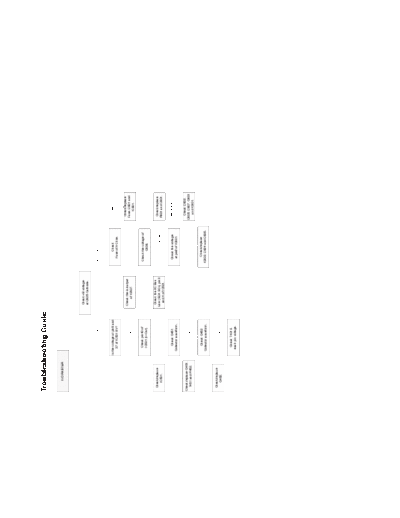
Troubleshooting Guide

      NO RASTER


                                                    Check +B voltage
                                                    at D825 Cathode.


                                    Normal                               Abnormal


                      Is the voltage at pin8 and                                Check                Open
                           37 of IC501 8V?                   No             Fuse of AC line.

                                                                                                   Check/replace
                                                   Check the in/output
                                    Yes                                             OK            Fuse, D801 and
                                                       of IC607.
                                                                                                      IC801.

                           Check pin40 of                                 Check the voltage of       0V
    No                     IC501 (H-Out).                                       C808.
                                                             OK

                                                    Check the IIC Bus
 Check/replace                                                                                     Check/replace
                                    Yes            Line (SDA,SCL) pin3              254~380V
    IC501.                                                                                        R801 and D801.
                                                      and 4 of IC501.

                            Check Q451                                     Check the voltage     Lower than 6V
    No                  Collector waveform.                                at pin9 of IC801.

                                                                                                   Check D802,
Check/replace Q451,
                                    Yes                                                          D805, D807, Q801
  T451 and R452.
                                                                                                    and IC801.

                            Check Q452                                       Check/replace
                        Collector waveform.                              IC803, D824 and D835.
    No

 Check/replace
    Q452.                           Yes


                           Check T401 &
                          each pin voltage.
         NO SOUND
       (PICTURE OK)


                            AM NO SOUND          NICAM,FM NO SOUND

                  No                               Check Sound        No
 Select correct            Check L System                                      Select correct
                                                  system in MENU
system in MENU                is right?                                      system in MENU.
                                                       OSD.

                                    Yes                     Yes

Check the logic of           Check the AM      Check demodulated             Check the logic of    OK      Check Z103,
 pin3 and 15 of                   Line.        SIF signal (pin26 of           pin3 and 15 of                   Q102
     IC101.        Abnor    (pin27 of IC101)         IC101).          Not         IC101.                 & pin25 of IC101.
                   mal                                                OK
                                     Normal       Normal                                     Not OK

             Not OK
                           Check AM Input of          Check                     Check C607              Check pin14
                             IC601, pin44.        pin47 of IC601.     Not        & R601.                & 25 of IC01.
                                                                      OK
             Not OK
  OK                                                OK
                                                            Normal

 Check/replace              Check/replace
 Z104 & +B of               pin14 & 25 of      Check X601 & pin16     Not OK        Check/replace
    IC101.                      IC01.          and 46 of IC601, IIC
                                                                                   X601 and IC601.
                                                    Bus Line.

                                                     OK                                       OK

                                                  Check R, L input    Not OK         Check R,L Out
                                                 of IC651, pin2 and
                                                                                       of IC601.
                                                         5.

                                                     OK                Not OK

                                                    Check +B of
                                                                            Is any OSD
                                                      IC651
                                                                             displayed?
                                                     & D822.
    NO PICTURE
     NO SOUND


                             Is any OSD displayed?


                        No                           Yes    Check receiving system in
        Go to
                                                             MENU & excute Auto-
NO RASTER (SOUND OK).
                                                                  programme.


       Go to                                               Does the Auto-programme
     NO SOUND.                                                operate properly?


                                                                         Not OK

                                                           Direct Input channel number
                                         Yes                & store in manual-program
                                                                      MENU.
                               Go to NO SOUND
                                                                                         Not OK   Check 5V, 12V,
                                PICTURE OK.                And Check 5V, 12V, 33V &                     33V
                                                            IIC Bus Line of TUNER.                & IIC Bus Line.
                                                                         OK

                                               OK              Is the CVBS signal
                                                              OK (pin 14 of IC101).

                                                                         Not OK

                                               OK
                                                              Check pin9 and 18 of
                                                                 MICOM IC01.

                                                                         Not OK

                                               OK                Check IC01 &
                                                                 H-Sync Line.
     NO RASTER
     (SOUND OK)


                                                                   Check the
                                                       Heater voltage of CPT(6-6.5Vrms).


         OK                       OK                                                              Not OK

      Check                                                                                        Check
                                    Check
HV,SCREEN voltage of                                                                       the HEATER pulse of FBT
                          lk Current of IC501,pin18.
      CPT.                                                                                         T401.


                                                                                             OK              Not OK

    OK            Check/replace         OK                                       Check                            Check
              CPT Board components.                                       FR405,FR901 & P402.                   FBT T401.


   Not OK                              Not OK

   Check/replace                  Check
    FBT T401.               P501,ZD564 & IC501.
NO PICTURE
 NO COLOR


   Is the CVBS signal at pin14 of
           IC101 normal?                                  No
                                            Check Receiving system in
                    Yes                    MENU & go to NO PICTURE,
                                                  NO SOUND.
   Is the CVBS signal at pin16 of
           IC201 normal?                                  No
                                          Check the state of pin11 and 13
                    Yes                   of IC201,L201 and R206(+B of
                                                     IC201).
   Is the CVBS signal at pin 13 of
           IC501 normal?                                  No

                                                 Check/replace
                    Yes
                                          Q201,L603(12V) & CVBS Line.

   Is the CVBS signal at pin 2 of
           IC702 normal?                                  No

                                            Check pin9 of IC501, IC702
                    Yes
                                              IIC Bus Line & Q701.

   Is the CVBS signal at pin11 of    No
           IC501 normal?

                    Yes

     Is the Y signal at pin 27 of
           IC501 normal?                                  No

                                                Check IC502, L542
                    Yes
                                                 & pin26 of IC501.
   Check if R-Y and B-Y signal of
    pin32 and 33 of IC501 are
                                                          No
              normal?
                                            Check X501, IC503, L541,
                                            ZD541 & IC504(In case of
                                               SECAM system).
      NO TELETEXT


    Check the voltage of     OK   Check CVBS signal at pin2    Not OK   Check/replace Q701, X701
 pin7, 16 and 21 of IC701.            of IC702 & X701.                          & IC501.


             0V                           OK


 Check 5V & 12V Supply       OK   Check IC701, 702 & IIC Bus
 Line of IC701 and 702.               Line (SDA, SCL).


And check pin803B & Power
    Line (MAIN2 PCB).
ADJUSTMENT INSTRUCTIONS
                                                                                  System      Frequency   Modulation    Output level   Adjust
YSafety Precautions                                                             B/G/SECAM-L     38.9MHz      OFF         10mVp-p       L107
  1. It is safe to adjust after using insulating transformer
                                                                                 SECAM-L'       33.9MHz      OFF         10mVp-p       VR102
     between the power supply line and chassis input to
     prevent the risk of electric shock and protect the
     instrument.                                                                                            (Table 1)
  2. Never disconnect leads while the TV receiver is on.
  3. Don't short any portion of circuits while power is on.
  4. The adjustment must be done by the correct appliances.                     T SECAM-L' Adjustment
     But this is changeable in view of productivity.
  5. Unless otherwise noted, set the line voltage to                              NOTE : This adjustment should be performed after PIF
     230Vac!10%, 50Hz.                                                                   adjustment.

YTest Equipment required                                                           Test Point     : TP1
  1.   RF signal generator (with pattern generator)
  2.   DC Power Supply                                                             Adjust         : VR102
  3.   Multimeter (volt meter)
  4.   Oscilloscope                                                               1) Turn on S1 and S3 and off S2.
  5.   Color analyzer                                                             2) Adjust VR101 so that the DC voltage may be indicated
                                                                                     3.1!0.1Vdc.

                      Main Board(Component side view)


                          V     Multimeter or Oscilloscope

Power-                                                 1
Supply
                                             IC01
 5V        JP7 IC05

 8V        JP4 IC102     TP1            24                          Signal-
                                                              103pF Generator
               5V                                    6 JP1          38.9MHz
                           L107                                     33.9MHz
                                                    10 JP2
               4.7k


◦ Jabse Service Manual Search 2024 ◦ Jabse PravopisonTap.bg ◦ Other service manual resources online : FixyaeServiceinfo