Service Manuals, User Guides, Schematic Diagrams or docs for : Philips Audio CDR779 CDR775_alim

<< Back | Home

Most service manuals and schematics are PDF files, so You will need Adobre Acrobat Reader to view : Acrobat Download Some of the files are DjVu format. Readers and resources available here : DjVu Resources
For the compressed files, most common are zip and rar. Please, extract files with Your favorite compression software ( WinZip, WinRAR ... ) before viewing. If a document has multiple parts, You should download all, before extracting.
Good luck. Repair on Your own risk. Make sure You know what You are doing.


Image preview - the first page of the document
CDR775_alim


>> Download CDR775_alim documenatation <<

Text preview - extract from the document
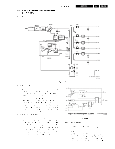
                                                                                                    Faultfinding Guide                                                CDR779                                8.           GB 59

8.2     Circuit description of the current mode
        power supply

8.2.1   Blockdiagram


                            Lightning                               Rectifier                                                                            6210
                            Protection                                                                                                    5131
                                                                                                                                                                                                                  +5V
                                                 EMI
            MAINS
                                                FILTER
                                                                                                                                 2
                                                                                                  2643


                                                                                                                                                         6230
                                                                                                                                                                                                                  +12V
                                                                                     Start         Overvoltage
                                                                                    Circuit        Protection       7            5


                                                     Comp                                Vcc                                                             6240
                                                                                                                    9                                                                                             -8V
                                                                                v
                                         2.5V                                                 t
                                                                  CLOCK
                                            Error                                                                                                        6250
                                            Amplifier              PWM                                              7125
                                                 +          Verror comparator                                                                                                                                     VFTD
                                                                    -                   S           Output
                                                 -                                   R      Q
                                                                    +                 latch                                                              6220
                                                                                                    Isense        Vsense                                                                                          VDC2

                                                 Vfb                                                              Rsense
                                                                CONTROL
                                                                                                                                                                                                                  VDC1


                                                                                                                           Vcc                    +12V +5V

                                                                                                                                           7131


                                                                                                                                                                                                                   0V
                                                                                                                                           7201


                                                                                                                                 REGULATION                                                      CL 06532151_018.eps
                                                                                                                                                                                                             271100


                                                                                                  Figure 8-10

8.2.2   Function description
                                                                                                                           7
                                                                                                                     VI

        MOSFET 7125 is used as a power switch controlled by the                                                                                   6V
                                                                                                                                             +
        controller IC 7110. When the switch is closed, energy is                                                                                                                            5V                             8
                                                                                                                                                                    S/R        REF                                             Vref
        transferred from mains to the transformer. This energy is                                                                            -
                                                                                                                            16V +
        supplied to the load when the switch is opened. Through                                                            5

        control of the switched-on time, the energy transferred in                                                 GND                                                     2.5V      BIAS


        each cycle is regulated so that the output voltages are                                                            4                                                                                               6
        independent of load or input voltage variations. The                                                       Rt/ct                   OSC                                                                1                OUTPUT

        controlling device UC3842 is an integrated pulse width                                                                 2.5V                                                              S
                                                                                                                                             ERROR AMP                         I SENSE COMP
        modulator. A clock signal initiates power pulses at a fixed                                                        2          +                  2R
                                                                                                                                                                                  -
        frequency. The termination of each output pulse occurs when                                                 Vfb               -
                                                                                                                                                                R         1V      +
                                                                                                                                                                                                 R

                                                                                                                           1
        a feedback signal of the inductor current reaches a threshold                                             COMP                                                                           LATCH

        set by the error signal. In this way the error signal actually                                           I sense
                                                                                                                           3

        controls the peak inductor current on cycle-by cycle basis.
                                                                                                                           Figure B : Blockdiagram UC3842                                                     CL 06532151_019.eps
8.2.3   Description of UC3842                                                                                                                                                                                             271100


        The input voltage Vcc(pin 7) is monitored by a comparator                                                                                                              Figure 8-11
        with hysteresis, enabling the circuit at 16V and disabling the
        circuit below 10V. The error amplifier compares a voltage                                                8.2.4            Start up sequence
        Vfb(pin 2) related to the output voltage of the power supply,
        with an internal 2.5V reference. The current sense                                                                        t1: Charging the capacitor at Vcc
        comparator compares the output of the error amplifier with                                                                C2129 wiil be charged via R3123 and R3134, C2133 and
        the switch current Isense(pin 3) of the power supply. The                                                                 C2111 via R3129. The output is switched off
        output of the current sense comparator resets a latch, which                                                              During t1.
        is set every cycle by the oscillator. The output stage is a                                                               t2: Charging of output capacitors
        totem pole, capable of driving a MOSFET directly                                                                          When the input voltage of the IC exceeds 14,5V, the circuit is
                                                                                                                                  enabled and starts to produce output pulses. The current
                                                                                                                                  consumption of the circuit increases to about 17mA,
                                                                                                                                  depending on the external loads of the IC. At first, the
 GB 60                 8.              CDR779                       Faultfinding Guide

              capacitor at the Vcc pin will discharge because the primairy                           becomes reversed. This results in a current flow through the
              auxiliary voltage, coming from winding7-9 is below the Vcc                             tranformer's secondary winding via the diodes, electrolytic
              voltage. At some moment during t2, the primary auxiliary                               capacitors and the load. This current is also ramp shaped but
              voltages reaches the same level as Vcc.                                                decreasing.
              This primary auxiliary voltage now determines the Vcc                                  TimeDEAD phase : when the stored energy has been
              voltage                                                                                supplied to the load, the voltage from the secondary windings
              t3: regulation                                                                         falls below the output voltage(held constant by the
              The output voltage of the power supply is in regulation                                electrolytic capacitors) plus the threshold voltage of the
              t4: overload                                                                           diodes. The current in the secondary winding stops flowing.
              When the output is shortened, the supply voltage of the                                At this point, the drain voltage of the MOSFET is not yet zero
              circuit will decrease and after some time drop below the                               because C2609 between drain and source contains a certain
              lower threshold voltage. At that moment, the output will be                            charge. This charge will start a sine-shaped ringing together
              disabled and the process of charging the Vcc capacitor starts                          with the transformer's self-induction.
              again. If the output is still shorted at the next t2 phase, the                        The oscillator will start a next cyclus which consists of the
              complete start-and stop sequence will repeat. The power                                described three phases. The time of the different phases
              supply comes in a hiccup mode.                                                         depends on the mains voltage and the load.
                                                                                                     TimeDEAD is maximum at an input of 400VDC and minimum
                                                                                                     load, it will be zero at an input of 100VDC and overload.
             16V
                       Vcc                                                                      V2
              12V

             10V                                                                         Vosc
                       Vc2134
                                                                                                V1
              0V

                                                                                                0

         20mA
                                                                                         Vcomp

                                                                                         Vsense
        Icc

             1mA


                                                                                         Vgate

        OUTPUT

                                                                                         Vdrain


                                                       short

        Vo                                                                               Idrain

         0
                        t1        t2          t3               t4
                                                                                         Idiodes

                    Figure C : Start-up sequence
                                                     CL 06532151_020.eps
                                                                 271100                               Ton   Tdiode Tdead                         CL 06532151_021.eps
                                                                                                                                                             271100


                                   Figure 8-12                                                                             Figure 8-13

8.2.5         Regulation

              Figure 4 shows the most relevant signals during the
              regulation phase of the power supply.
              The oscillator voltage ramps up and down between V1 and
              V2. The voltage at the current sense terminal is compared
              every cycle with the output of the error amplifier Vcomp. The
              output is switched off when the current sense level exceeds
              the level at the output of the error amplifier.
              TimeON phase : A drain current will flow from the positive
              supply at pin 1 through the transformer's primary winding, the
              MOSFET and Rsense to ground. As the positive voltage at
              pin 1 of the transformer is constant, the current will increase
              linearly and create a ramp dependent on the mains voltage
              and the inductance of the primary winding. A certain amount
              of energy is stored in the transformer in the form of a
              magnetic field. The polarity of the voltages at the secundary
              windings is such that the diodes are non-conducting.
              TimeDIODE phase : When the MOSFET is switched off,
              energy is no longer supplied to the tranformer. The
              inductance of the tranformer now tries to maintain the current
              which has been flowing through it at a constant level. The
              polarity of the voltage from the transformer therefore
                                                                     Faultfinding Guide              CDR779                   8.       GB 61

8.2.6     Oscillograms                                                     8.2.7   Circuit description

                                                                                   Input circuit
        Oscillograms                                                               The input circuit consists of a lightning protection circuit and
                                                                                   an EMI filter.
                                                                                   The lightning protection comprises R3120, gasarrestor 1125
                              CH1 2                                                and R3124.
                              CH2                                                  The EMI filter is formed by C2120, L5120, C2125 and R3124.
                PM3394B       CH3 2 V~ ALT MTB5.00us- 0.90dv ch1-                  It prevents inflow of noise into/from the mains.
         ch1
                 1                                                                 Primary rectifier/smoothing circuit
         ch3                                                                       The AC input is rectified by rectifier bridge 6102 and
                                                                                   smoothed into C2121. The voltage over C2121 is
                    T
         ch2                                                                       approximately 300V. It can vary from 100V to 390V.

                 3                                                                 Start circuit and Vcc supply
                                                                                   This circuit is formed by R3123, R3134, C2129, D6129,
                                                                                   R3129, R3111, C2133 and C2111.
                                                                                   When the power plug is connected to the mains voltage, the
                                                                                   stabilised voltage over D6129(24V) will charge C2133 via
                                                                                   R3129. When the voltage reaches 14,5V across C2111, the
                                                                                   control circuit of IC7110 is turned on and the regulation
                2                                                                  starts. During regulation, Vcc of IC7110 will be supplied by
                                                                                   the rectified voltage from winding 7-9 via L5132, D6132 and
                                                                                   C2133.
        ch1 : Drain voltage
        ch2 : Drain current                                                        Control circuit
        ch3 : Gate voltage                                                         The control circuit exists of IC7110, C2102, C2104, C2107,
                                                                                   C2109, C2110, R3102, R3103, R3104, R3107, R3108,
                              CH1 1                                                R3109 and R3110. C2102 and R3110 define the frequency
                PM3394B       CH3 50mV~ ALT MTB5.00us- 0.90dv ch1-                 of the oscillator.
         ch1
                                                                                   Power switch circuit
                    1
         ch3                                                                       This circuit comprises MOSFET 7125, Rsense 3126, 3127
                                                                                   and 3128, R3125, C2127, L5125, R3112 and R3113. R3125
                    T
                                                                                   is a pull-down resistor to remove static charges from the gate
                                                                                   of the MOSFET.

                                                                                   Regulation circuit
                    3                                                              The regulation circuit comprises opto-coupler 7200 which
                                                                                   isolates the error signal from the control IC on the primary
                                                                                   side and a reference component 7201. The TL431(7201) can
                                                                                   be represented by two components:


◦ Jabse Service Manual Search 2024 ◦ Jabse PravopisonTap.bg ◦ Other service manual resources online : FixyaeServiceinfo