Service Manuals, User Guides, Schematic Diagrams or docs for : Philips Audio BTM3160 service
<< Back | HomeMost service manuals and schematics are PDF files, so You will need Adobre Acrobat Reader to view : Acrobat Download Some of the files are DjVu format. Readers and resources available here : DjVu Resources
For the compressed files, most common are zip and rar. Please, extract files with Your favorite compression software ( WinZip, WinRAR ... ) before viewing. If a document has multiple parts, You should download all, before extracting.
Good luck. Repair on Your own risk. Make sure You know what You are doing.
Image preview - the first page of the document
>> Download service documenatation <<
Text preview - extract from the document
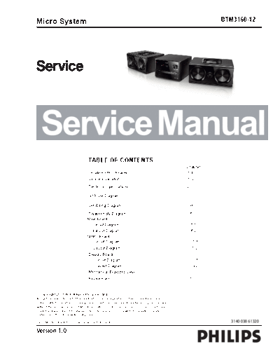
Micro System                                                                                                                      BTM3160/12


                                     TABLE OF CONTENTS
                                                                                                                Chapter
                                     Location of PC Boards ......................................................1-1
                                     Versions Variation ..............................................................1--2

                                     Technical Specications ......................................................2

                                    Set Block Diagram.................................................................33

                                     Set Wiring Diagram ...............................................................44

                                    Disassembly Diagram ...........................................................55
                                    Main Board
                                      Circuit Diagram ..................................................................6-1
                                        Layout Diagram..................................................................6-2
                                    SMPS Board
                                      Circuit Diagram...................................................................7-1
                                         Layout Diagram..................................................................7-22
                                     Display Board
                                        Circuit Diagram..................................................................8-1
                                        Layout Diagram ................................................................8-28-2
                                     Mechanical Exploded View ....................................................9
                                     Revision list ..........................................................................10


Published by Kelly & Xu wk1352 Subject to modification                                                                              3140 038 61320
 1-1.Location of PC Board


                   47
                  5


                   7


1-2.Versions Variation


                      Type/Version           BTM3160
                                      /12
  Board in used      Service Policy
                                      (EU)
  Main board                          M
  SMPS board                          M
  Display board                       M


 Tips: C--Component Level Repair
       M--Module Level Rpair
                                              2.T2.Technical Specications

module:BTM3160


TEST CONDITIONS:
1.POWER SUPPLY: AC.Accordiing to Ver
2.REF OUTPUT: 6  1W , Sound effect off
3.FM MONO: 22.5KHz Dev,1KHz MODULATION ,75 IMPEDANCE ,60dBu
4.FM STEREO : MAIN+SUB = 50KHz, PILOT : 10KHz,COMPOSITE: 40.0KHz
FM SECTION
                                                                                     TEST DATA
NO                     TEST ITEMS                           UNIT   NOM.   LIMIT
                                                                                    1#        2#
                                                                           87.5    87.5      87.5
 1              Fvequency Range                             MHz
                                                                           108     108       108
                                                   90.1             16      22       16       16
 2        26dB QUENTING SENSITIVITY                98.1     dBf     16      22       16       15
                                                   106.1            16      22       16       16
 3             -3dB LIMITING POINT                          dBf     20      26       12       12
 3      FM IF REJECTION 98MHZ S/N=26dB                      dB      65      60      110       110
 4       IMAGE REJECT 98MHZ S/N=26dB                        dB      40      25      110       110
                                                  MONO              50      45       68       69
 5                    S/N                                   Db
                                                   ST               50      45       64       64
 6           OVERALL DISTERTION                              %      2       5       0.2       0.2
 7            MODULATION HUM                                dB      50      45       57       57
                                                 90.1MHz    dBf     _     16-36      20       20
 9               TUNING SENS                     98.1MHz    dBf     _     16-36      20       20
                                                 106.1MHz   dBf     _     16-36      20       20
 10      STREO CHANNEL SEPARATION                  1KHz     dB      25      18       39       38
 11           THD 10% POWER                        1KHz     W       _     6
◦ Jabse Service Manual Search 2026 ◦ Jabse Pravopis ◦ onTap.bg ◦ Other service manual resources online : Fixya ◦ eServiceinfo