Service Manuals, User Guides, Schematic Diagrams or docs for : Philips Audio DTB3185 service
<< Back | HomeMost service manuals and schematics are PDF files, so You will need Adobre Acrobat Reader to view : Acrobat Download Some of the files are DjVu format. Readers and resources available here : DjVu Resources
For the compressed files, most common are zip and rar. Please, extract files with Your favorite compression software ( WinZip, WinRAR ... ) before viewing. If a document has multiple parts, You should download all, before extracting.
Good luck. Repair on Your own risk. Make sure You know what You are doing.
Image preview - the first page of the document
>> Download service documenatation <<
Text preview - extract from the document
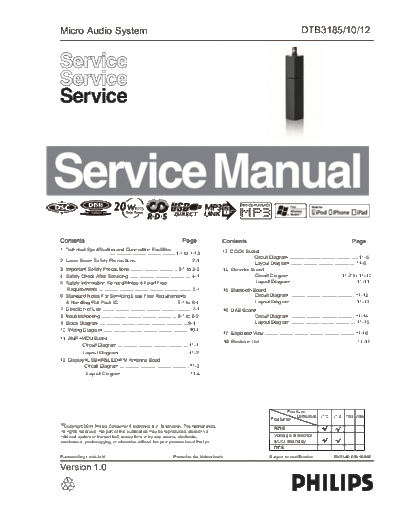
Micro Audio System                                                                                                                                   DTB3185/10/12


Contents                                                                    Page                Contents                                                                             Page
1 Technical Specification and Connection Facilities                                             13 DOCK Board
                       .................................................1-1 to 1-13
                                                                                                            Circuit Diagram ...................................................11-5
2 Laser Beam Safety Precautions......................................... 2-1                                Layout Diagram ............................................... 11-6
3 Important Safety Precautions .................................. 3-1 to 3-2                    14 Decoder Board
4 Safety Check After Servicing ............................................. 4-1                            Circuit Diagram ..................................... 11-7 to 11-10
5 Safety Information General Notes & Lead Free                                                              Layout Diagram ............................................... 11-11
   Requirements .................................................................... 5-1        15 Bluetooth Board
6 Standard Notes For Servicing,Lead Free Requirements                                                        Circuit Diagram ............................................... 11-12
  & Handling Flat Pack IC .......................................... 6-1 to 6-4                               Layout Diagram ............................................... 11-13
7 Direction of Use ................................................................. 7-1        16 DAB Board
8 Troubleshooting ....................................................... 8-1 to 8-2                        Circuit Diagram ............................................... 11-14
9 Block Diagram .................................................................9-1                        Layout Diagram ............................................... 11-15
10 Wiring Diagram ...............................................................10-1
                                                                                                17 Exploded View...................................................................11-16
11 AMP+MCU Board
                                                                                                    18 Revision List .......................................................................11-17
       Circuit Diagram ....................................................11-1
          Layout Diagram ...................................................11-2
12 Display+USB+IR&LED+FM Antenna Boad
           Circuit Diagram ...................................................11-3
                Layout Diagram ..................................................11-4


                                                                                                                                            Feature
                                                                                                                                               Different /10              /12    /93 /96
                                                                                                                                 Features
◦ Jabse Service Manual Search 2026 ◦ Jabse Pravopis ◦ onTap.bg ◦ Other service manual resources online : Fixya ◦ eServiceinfo