Service Manuals, User Guides, Schematic Diagrams or docs for : Philips Audio HTS5500C HTS5500
<< Back | HomeMost service manuals and schematics are PDF files, so You will need Adobre Acrobat Reader to view : Acrobat Download Some of the files are DjVu format. Readers and resources available here : DjVu Resources
For the compressed files, most common are zip and rar. Please, extract files with Your favorite compression software ( WinZip, WinRAR ... ) before viewing. If a document has multiple parts, You should download all, before extracting.
Good luck. Repair on Your own risk. Make sure You know what You are doing.
Image preview - the first page of the document
>> Download HTS5500 documenatation <<
Text preview - extract from the document
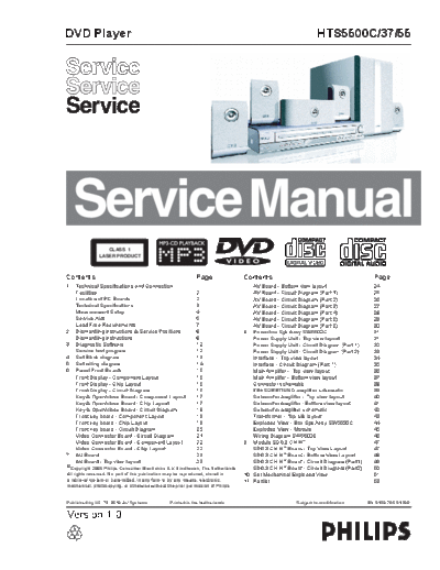
DVD Player                                                                                                      HTS5500C/37/55


                 CLASS 1
              LASER PRODUCT


Contents                                                   Page                   Contents                                            Page
1   Technical Specifications and Connection                                          AV Board - Bottom view layout                    24
    Facilities                                             2                         AV Board - Circuit Diagram (Part 1)              25
    Location of PC Boards                                  2                         AV Board - Circuit Diagram (Part 2)              26
    Technical Specifications                               3                         AV Board - Circuit Diagram (Part 3)              27
    Measurement Setup                                      4                         AV Board - Circuit Diagram (Part 4)              28
    Service Aids                                           5                         AV Board - Circuit Diagram (Part 5)              29
    Lead Free Requirements                                 7                         AV Board - Circuit Diagram (Part 6)              30
2   Dismantling instructions & Service Positions           8                      8 Powerbox Spk Assy SW5500C                         31
    Dismantling instructions                               8                         Power Supply Unit - Top view layout              31
3   Diagnostic Software                                    10                        Power Supply Unit - Circuit Diagram (Part 1)     32
    Service test program                                   10                        Power Supply Unit - Circuit Diagram (Part 2)     33
4   Set Block diagram                                      13                        Interface - Top view layout                      34
5   Set wiring diagram                                     14                        Interface - Circuit Diagram (Part 1)             35
6   Panel Front Boards                                     15                        Main Amplifer - Top view layout                  36
    Front Display - Component Layout                       15                        Main Amplifer - Bottom view layout               37
    Front Display - Chip Layout                            15                        Connector schematic                              38
    Front Display - Circuit Diagram                        16                        FR+SURROUND amplifier schematic                  39
    Key & Open/close Board - Component Layout              17                        Subwoofer Amplifer - Top view layout             40
    Key & Open/close Board - Chip Layout                   17                        Subwoofer Amplifer - Bottom view layout          41
    Key & Open/close Board - Circuit Diagram               18                        Subwoofer amplifier schematic                    42
    Front key board - Component Layout                     19                        Transformer - Top silk layout                    43
    Front key board - Chip Layout                          19                        Exploded View - Box Spk Assy SW5500C             44
    Front key board - Circuit Diagram                      20                        Exploded View - Module                           45
    Video Connector Board - Circuit Diagram                21                        Wiring Diagram SW5500C                           46
    Video Connector Board - Component Layout               22                     9 Module SD6.3 CH HT                                47
    Video Connector Board - Chip Layout                    22                        SD6.3 CH HT Board - Top View Layout              47
7   AV Board                                               23                        SD6.3 CH HT Board - Bottom View Layout           48
    AV Board - Top view layout                             23                        SD6.3 CH HT Board - Circuit Diagram (Part1)      49
◦ Jabse Service Manual Search 2026 ◦ Jabse Pravopis ◦ onTap.bg ◦ Other service manual resources online : Fixya ◦ eServiceinfo