Service Manuals, User Guides, Schematic Diagrams or docs for : Philips Audio HTS8000 HTS8000S69_ET-SB-EX-SI_1186036614
<< Back | HomeMost service manuals and schematics are PDF files, so You will need Adobre Acrobat Reader to view : Acrobat Download Some of the files are DjVu format. Readers and resources available here : DjVu Resources
For the compressed files, most common are zip and rar. Please, extract files with Your favorite compression software ( WinZip, WinRAR ... ) before viewing. If a document has multiple parts, You should download all, before extracting.
Good luck. Repair on Your own risk. Make sure You know what You are doing.
Image preview - the first page of the document
>> Download HTS8000S69_ET-SB-EX-SI_1186036614 documenatation <<
Text preview - extract from the document
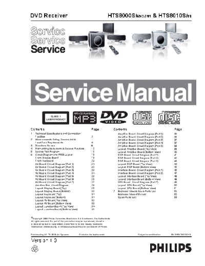
DVD Receiver                                                                HTS8000S/69/37/01 & HTS8010S/01


                 CLASS 1
              LASER PRODUCT


Contents                                                   Page                   Contents                                          Page
1   Technical Specifications and Connection                                           Amplifier Board: Circuit Diagram (Part 1)     36
    Facilities                                             2                          Amplifier Board: Circuit Diagram (Part 2)     36
2   Measurements Setup, Service Aid &                                                 Amplifier Board: Circuit Diagram (Part 3)     37
    Lead Free Requirements                                 4                          Amplifier Board: Circuit Diagram (Part 4)     37
3   Directions for use                                     8                          Amplifier Board: Circuit Diagram (Part 5)     38
4   Dismantling Instructions & Service Positions           10                         Layout: Amplifier Board (Top View)            39
5   Service Test Program                                   15                         Layout: Amplifier Board (Bottom View)         40
6   Circuit Diagram and PWB Layout                         19                         DSP Board: Circuit Diagram (Part 1)           41
    Front: Display Board                                   19                         DSP Board: Circuit Diagram (Part 2)           42
    Front: Keyboard                                        20                         DSP Board: Circuit Diagram (Part 3)           43
    AV Board: Circuit Diagram (Part 1)                     21                         Layout: DSP Board (Top View)                  44
    AV Board: Circuit Diagram (Part 2)                     22                         Layout: DSP Board (Bottom View)               45
    AV Board: Circuit Diagram (Part 3)                     23                         Interface Board: Circuit Diagram (Part 1)     46
    AV Board: Circuit Diagram (Part 4)                     24                         Interface Board: Circuit Diagram (Part 2)     47
    AV Board: Circuit Diagram (Part 5)                     25                         Layout: Interface Board (Top View)            48
    AV Board: Circuit Diagram (Part 6)                     26                         Layout: Interface Board (Bottom View)         48
    AV Board: Circuit Diagram (Part 7)                     27                         SPK Board: Circuit Diagram (Part 1)           49
    Junction Box: Circuit Diagram                          28                         Layout: SPK Board (Top View)                  50
    Layout: Display Board (Top)                            29                         Layout: SPK Board (Bottom View)               51
    Layout: Display Board (Bottom)                         30                     7   Exploded View & Spare Parts List              52
    Layout: Keyboard (Top)                                 31                         Exploded View of the set                      52
    Layout: Keyboard (Bottom)                              31                         Spare Parts List                              53
    Layout: AV Board (Top View)                            32
    Layout: AV Board (Bottom View)                         33
    Layout: Junction Board (Top View)                      34
    Layout: Junction Board (Bottom View)                   35
◦ Jabse Service Manual Search 2026 ◦ Jabse Pravopis ◦ onTap.bg ◦ Other service manual resources online : Fixya ◦ eServiceinfo