Service Manuals, User Guides, Schematic Diagrams or docs for : Philips LCD TV (and TPV schematics) 42PF333110 42PF3331_10_with_complete_LCD_boards.part14

<< Back | Home

Most service manuals and schematics are PDF files, so You will need Adobre Acrobat Reader to view : Acrobat Download Some of the files are DjVu format. Readers and resources available here : DjVu Resources
For the compressed files, most common are zip and rar. Please, extract files with Your favorite compression software ( WinZip, WinRAR ... ) before viewing. If a document has multiple parts, You should download all, before extracting.
Good luck. Repair on Your own risk. Make sure You know what You are doing.


Image preview - the first page of the document
42PF3331_10_with_complete_LCD_boards.part14


>> Download 42PF3331_10_with_complete_LCD_boards.part14 documenatation <<

Text preview - extract from the document
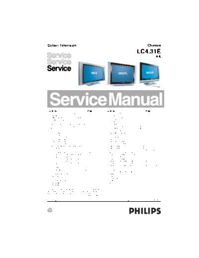
Colour Television                                                                                                                            Chassis
                                                                                                                                LC4.31E
                                                                                                                                                        AA


                                                                ME6                                  ME5FL                                 ME5P


                                                                                                                                                  G_16212_000.eps
                                                                                                                                                          191006


Contents                                                   Page                   Contents                                                 Page
1. Technical Specifications, Connections, and Chassis                                   SSB: Scaler Interface                         (B9) 60      74-83
   Overview                                        2                                    SSB: SDRAM                                   (B10) 61      74-83
2. Safety Instructions, Warnings, and Notes        5                                    SSB: Flash / Control                         (B11) 62      74-83
3. Directions for Use                              7                                    SSB: HDMI                                    (B12) 63      74-83
4. Mechanical Instructions                         8                                    SSB: MUX-Sync Interface                     (B13) 64       74-83
5. Service Modes, Error Codes, and Fault Finding 13                                     SSB: Digital I/O                             (B14) 65      74-83
6. Block Diagrams, Test Point Overviews, and                                            SSB: SCART Analog I/O                      (B15A) 66       74-83
   Waveforms                                                                            SSB: DMMI                                  (B15B) 67       74-83
   Wiring Diagram 26" & 32"                        23                                   SSB: Top Connectors                          (B16) 68      74-83
   Wiring Diagram 37"                              24                                   SSB: Side Connectors                         (B17) 69      74-83
   Wiring Diagram 42"                              25                                   SSB: ADC                                     (B18) 70      74-83
   Block Diagram Supply 37"                        26                                   SSB: Columbus                                (B19) 71      74-83
   Block Diagram Supply 42"                        27                                   SSB: Pacific 3                               (B20) 72      74-83
   Block Diagram Video                             28                                   SSB: Diversity Tables B9-B20                        73
   Block Diagram Audio                             29                                   Class D Audio Amplifier (26" & 32")            (C) 84      85
   Test Point Overview Small Signal Board          30                                   Side I/O Panel (26" & 32")                     (D) 86      87
   I2C Overview                                    31                                   Side I/O Panel (37" & 42")                     (D) 88      89
   Supply Voltage Overview                         32                                   Keyboard Control Board (26" & 32")             (E) 90      90
7. Circuit Diagrams and PWB Layouts                Diagram           PWB                Keyboard Control Board (37" & 42")             (E) 91      91
   LCD Supply (37"): Mains Filter & Standby (A1) 33                  35-40              Front IR / LED Panel (26" & 32") (ME5P)         (J) 92     92
   LCD Supply (37"): Supply                   (A2) 34                35-40              IR-LED and Light Sensor Panel (26"& 32") (J) 93            93
   LCD Supply (42"): Mains Filter + Stdby A (A1) 41                  45-50              Front IR / LED Panel (37" & 42")                (J) 94     95
   LCD Supply (42"): Supply A                 (A2) 42                45-50              Standby & Audio Panel: Connections          (SA1) 96       99-101
   LCD Supply (42"): Mains Filter + Stdby B (A3) 43                  45-50              Standby & Audio Panel: Standby              (SA2) 97       99-101
   LCD Supply (42"): Supply B                 (A4) 44                45-50              Standby & Audio Panel: Audio                (SA3) 98       99-101
   SSB: Tuner and IF                          (B1) 51                74-83              OTC Flash (For 1000pg TXT)                     (T) 102     103
   SSB: Hercules                              (B2) 52                74-83        8.    Alignments                                          105
   SSB: Sync Interface                        (B3) 53                74-83        9.    Circuit Descriptions, Abbreviation List, and IC Data
   SSB: Audio Delay Line (PDP Only)           (B4) 54                74-83              Sheets                                              110
   SSB: Audio Processing                      (B5) 55                74-83              Abbreviation List                                   111
   SSB: DC-DC Converter                       (B6) 56                74-83              IC Data Sheets                                      114
   SSB: Diversity Tables B1-B6                     57                             10.   Spare Parts List                                    118
   SSB: Scaler                                (B7) 58                74-83        11.   Revision List                                       129
   SSB: Scaler                                (B8) 59                74-83


◦ Jabse Service Manual Search 2024 ◦ Jabse PravopisonTap.bg ◦ Other service manual resources online : FixyaeServiceinfo