Service Manuals, User Guides, Schematic Diagrams or docs for : Philips LCD TV (and TPV schematics) 32PFL7762D12 philips_ch.lc7.5e-la-32pfl7762d-12

<< Back | Home

Most service manuals and schematics are PDF files, so You will need Adobre Acrobat Reader to view : Acrobat Download Some of the files are DjVu format. Readers and resources available here : DjVu Resources
For the compressed files, most common are zip and rar. Please, extract files with Your favorite compression software ( WinZip, WinRAR ... ) before viewing. If a document has multiple parts, You should download all, before extracting.
Good luck. Repair on Your own risk. Make sure You know what You are doing.


Image preview - the first page of the document
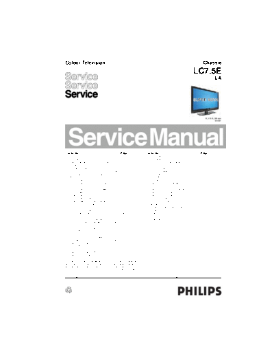
philips_ch.lc7.5e-la-32pfl7762d-12


>> Download philips_ch.lc7.5e-la-32pfl7762d-12 documenatation <<

Text preview - extract from the document
Colour Television                                                                                                                           Chassis
                                                                                                                                    LC7.5E
                                                                                                                                                          LA


                                                                                                                                    SUPER NOVA


                                                                                                                                                 H_17370_000.eps
                                                                                                                                                         041007


Contents                                                   Page                   Contents                                                Page
1. Technical Specifications, Connections, and Chassis                                   SSB: Audio Processor                      (B06A) 58           67-76
   Overview                                        2                                    SSB: Audio                                (B06B) 59           67-76
2. Safety Instructions, Warnings, and Notes        6                                    SSB: Headphone Ampl. & Muting             (B06C) 60           67-76
3. Directions for Use                              7                                    SSB: YPBPR & SVHS                         (B07A) 61           67-76
4. Mechanical Instructions                         8                                    SSB: I/O SCART 1&2                        (B07B) 62           67-76
5. Service Modes, Error Codes, and Fault Finding 15                                     SSB: HDMI Main                            (B07C) 63           67-76
6. Block Diagrams, Test Point Overviews, and                                            SSB: HDMI Switch                          (B07D) 64           67-76
   Waveforms                                                                            SSB: LVDS Connector                       (B07E) 65           67-76
   Wiring Diagram 32" LCD (ME7)                    29                                   SSB: SRP List                                      66         67-76
   Wiring Diagram 32" LCD with AmbiLight (ME7) 30                                       Side I/O Panel (32"): HDMI                    (D) 77          79
   Wiring Diagram 42" LCD (ME7)                    31                                   Side I/O Panel (32")                          (D) 78          79
   Wiring Diagram 42" LCD with AmbiLight (ME7) 32                                       Side I/O Panel (42" & 52"): HDMI              (D) 80          82
   Wiring Diagram 52" LCD (ME7)                    33                                   Side I/O Panel (42" & 52")                    (D) 81          82
   Block Diagram Video                             34                                   Side I/O Panel (42" & 52")                    (D) 81          82
   Block Diagram Audio                             35                                   Keyboard Control Panel                        (E) 83          84
   Block Diagram Control & Clock Signals           36                                   Front IR / LED Panel                           (J) 85         86
   Testpoint Overview SSB (Bottom Side)            37-41                          8.    Alignments                                         87
   I2C Overview                                    42                             9.    Circuit Descriptions, Abbreviation List, and IC Data
   Supply Lines Overview                           43                                   Sheets                                             92
7. Circuit Diagrams and PWB Layouts                Diagram           PWB                Abbreviation List                                  97
   SSB: DC / DC 3V3, VTUN, & 5V_SW (B01A) 44                         67-76              IC Data Sheets                                     99
   SSB: DC / DC 1V2, 2V5, & 1V8            (B01B) 45                 67-76        10.   Spare Parts List                                   107
   SSB: Tuner IF & Demodulator               (B02) 46                67-76        11.   Revision List                                      133
   SSB: DVB-Demodulator                    (B03A) 47                 67-76
   SSB: DVB-T: DVB Common Interface (B03B) 48                        67-76
   SSB: DVB MOJO                           (B03C) 49                 67-76
   SSB: DVB MOJO Memory                    (B03D) 50                 67-76
   SSB: DVB MOJO Analog Back End           (B03E) 51                 67-76
   SSB: Micro Processor                      (B04) 52                67-76
   SSB: Trident WX68                       (B05A) 53                 67-76
   SSB: DDR & CPU Interface                (B05B) 54                 67-76
   SSB: WX Power / Ground                  (B05C) 55                 67-76
   SSB: FPGA Interface (AL Sets only)      (B05D) 56                 67-76
   SSB: FPGA I/O Banks                     (B05E) 57                 67-76


◦ Jabse Service Manual Search 2024 ◦ Jabse PravopisonTap.bg ◦ Other service manual resources online : FixyaeServiceinfo