Service Manuals, User Guides, Schematic Diagrams or docs for : Philips LCD TV (and TPV schematics) LC03A aa LC03AAA_ET-SB-BA-SI_1219316114
<< Back | HomeMost service manuals and schematics are PDF files, so You will need Adobre Acrobat Reader to view : Acrobat Download Some of the files are DjVu format. Readers and resources available here : DjVu Resources
For the compressed files, most common are zip and rar. Please, extract files with Your favorite compression software ( WinZip, WinRAR ... ) before viewing. If a document has multiple parts, You should download all, before extracting.
Good luck. Repair on Your own risk. Make sure You know what You are doing.
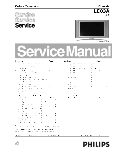
Image preview - the first page of the document

>> Download LC03AAA_ET-SB-BA-SI_1219316114 documenatation <<
Text preview - extract from the document
Colour Television                                                                                                                       Chassis
                                                                                                                                   LC03A
                                                                                                                                                 AA


Contents                                                   Page                   Contents                                          Page
1   Technical Specifications, Connections,                                            Scaler Panel: Video Decoder      (Diagram C3)    88       96-105
    and Chassis Overview                                   2                          Scaler Panel: Scaler             (Diagram C4)    89       96-105
2   Safety Instructions, Warnings, and Notes               5                          Scaler Panel: Output (LVDS)      (Diagram C5)    90       96-105
3   Directions for Use                                     6                          Scaler Panel: SDRAM (Scaler)     (Diagram C6)    91       96-105
4   Mechanical Instructions                                30                         Scaler Panel: PC-In              (Diagram C7)    92       96-105
5   Service Modes, Error Messages,                                                    Scaler Panel: uP                 (Diagram C8)    93       96-105
    and Repair Tips                                        36                         Scaler Panel: Video Converter    (Diagram C9)    94       96-105
6   Block Diagrams                                                                    Scaler Panel: HDTV Decoder       (Diagram C10)   95       96-105
    Block Diagram (Tuner-IF-Video)                         43                         Side I/O Panel                   (Diagram D)     106      107
    Block Diagram (TV Control and Inverter Panel)          44                         Top Control                      (Diagram E)     106      108
    Block Diagram (Scaler Board)                           45                         Inverter Panel (TN)              (Diagram IN)    109      110
    I2C-IC's and Error Codes Overview                      46                         Inverter Panel (IPS)             (Diagram IN1)   111      113
    Powerlines Overview                                    47                         Inverter Panel (IPS)             (Diagram IN2)   112      113
    Testpoint Overview TV Board (15"/17")                  48                         Front LED Panel                  (Diagram J)     114      114
    Mapping Testp. and Waveforms TV/Scaler                 49                      8 Alignments                                        115
    Testpoint Overview Scaler Board                        50                      9 Circuit Descriptions                              119
    Testpoint Overview TV Board (23")                      51                         Abbreviation List                                131
    Wiring Diagram 15 & 17 Inch                            52                         IC Data Sheets                                   133
    Wiring Diagram 23 Inch Wide Screen                     53                      10 Spare Parts List                                 136
7   Electrical Diagrams and PWB lay-outs                   Diagram   PWB           11 Revision List                                    143
    TV Board: U_Cont                (Diagram A1)           54        66-85
    TV Board: Mem for 100-pg Txt (Diagram A2)              55        66-85
    TV Board: Tuner Function        (Diagram A3)           56        66-85
    TV Board: IF Video Sync Chr. (Diagram A4)              57        66-85
    TV Board: SAW Filter            (Diagram A5)           58        66-85
    TV Board: Analog Comb Filter (Diagram A6)              59        66-85
    TV Board: Audio Delay Line      (Diagram A7)           60        66-85
    TV Board: Audio Processing      (Diagram A8)           61        66-85
    TV Board: Audio Ampl. (15"/17")(Diagram A9a)           62        66-85
    TV Board: Audio Amplifier (23") (Diagram A9b)          63        66-85
    TV Board: Local Supply          (Diagram A10)          64        66-85
    TV Board: Cinch I/O             (Diagram A11)          65        66-85
    Scaler Panel: Power             (Diagram C1)           86        96-105
    Scaler Panel: I/O & Interface   (Diagram C2)           87        96-105
◦ Jabse Service Manual Search 2024 ◦ Jabse Pravopis ◦ onTap.bg ◦ Other service manual resources online : Fixya ◦ eServiceinfo