Service Manuals, User Guides, Schematic Diagrams or docs for : Philips LCD TV (and TPV schematics) LC4.8L la LC4.8L

<< Back | Home

Most service manuals and schematics are PDF files, so You will need Adobre Acrobat Reader to view : Acrobat Download Some of the files are DjVu format. Readers and resources available here : DjVu Resources
For the compressed files, most common are zip and rar. Please, extract files with Your favorite compression software ( WinZip, WinRAR ... ) before viewing. If a document has multiple parts, You should download all, before extracting.
Good luck. Repair on Your own risk. Make sure You know what You are doing.


Image preview - the first page of the document
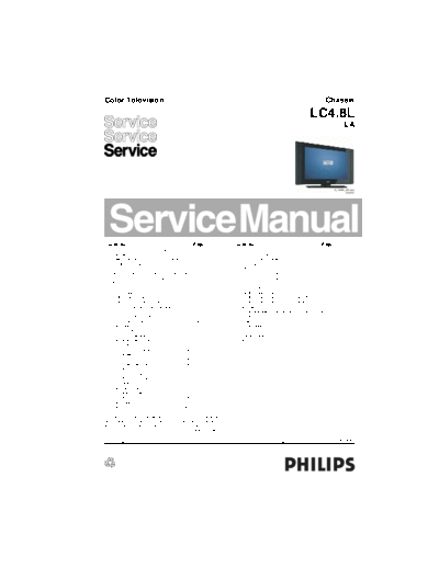
LC4.8L


>> Download LC4.8L documenatation <<

Text preview - extract from the document
Color Television                                                                                                                             Chassis
                                                                                                                                     LC4.8L
                                                                                                                                                         LA


                                                                                                                                            ME6


                                                                                                                                                  H_16980_000.eps
                                                                                                                                                          200207


Contents                                                   Page                   Contents                                                 Page
1. Technical Specifications, Connections, and Chassis                                   SSB: EPLD                                   (B21) 43        45-54
   Overview                                        2                                    SSB: Cinch Analog I/O                       (B23) 44        45-54
2. Safety Instructions, Warnings, and Notes        4                                    Class D Audio Amplifier (32")                 (C) 55        56
3. Directions for Use                              5                                    Layout Side I/O Panel (32") (Top Side)        (D) 57        58
4. Mechanical Instructions                         6                                    Side I/O Panel (37" & 42")                    (D) 59        60
5. Service Modes, Error Codes, and Fault Finding 11                                     Keyboard Control Board (32")                   (E) 61       61
6. Block Diagrams, Test Point Overviews, and                                            Keyboard Control Board (37" & 42")             (E) 62       62
   Waveforms                                                                            IR/LED Panel (32" & 37")                        (J) 63      63
   Wiring Diagram 32"                              17                                   IR / LED Panel (42")                            (J) 64      64
   Wiring Diagram 37" & 42"                        18                                   Standby/Audio Panel (37" & 42"): Conn. (SA1) 65             68- 70
   Block Diagram Video                             19                                   Standby/Audio Panel (37" & 42"): Standby(SA2) 66            68- 70
   Block Diagram Audio & Control                   20                                   Standby/Audio Panel (37" & 42"): Audio (SA3) 67             68- 70
   Test Point Overview SSB (Top Side)              21                             8.    Alignments                                          71
   I2C Overview                                    22                             9.    Circuit Descriptions, Abbreviation List, and IC Data
   Supply Voltage Overview                         23                                   Sheets                                              75
7. Circuit Diagrams and PWB Layouts                Diagram           PWB                Abbreviation List                                   81
   SSB: Tuner and IF                          (B1) 24                45-54              IC Data Sheets                                      83
   SSB: Hercules                              (B2) 25                45-54        10.   Spare Parts List                                    87
   SSB: Sync Interface                        (B3) 26                45-54              Diversity Table SSB                                 87
   SSB: Audio Delay Line (PDP Only)           (B4) 27                45-54        11.   Revision List                                       93
   SSB: Audio Processing                      (B5) 28                45-54
   SSB: DC-DC Converter                       (B6) 29                45-54
   SSB: Scaler                                (B7) 30                45-54
   SSB: Scaler                                (B8) 31                45-54
   SSB: Scaler Interface                      (B9) 32                45-54
   SSB: SDRAM                               (B10) 33                 45-54
   SSB: Flash / Control                     (B11) 34                 45-54
   SSB: MUX-Sync Interface                  (B13) 36                 45-54
   SSB: Digital I/O                         (B14) 37                 45-54
   SSB: Top Connectors                      (B16) 38                 45-54
   SSB: Side Connectors                     (B17) 39                 45-54
   SSB: ADC                                 (B18) 40                 45-54
   SSB: Columbus                            (B19) 41                 45-54
   SSB: EPLD                                (B20) 42                 45-54


◦ Jabse Service Manual Search 2024 ◦ Jabse PravopisonTap.bg ◦ Other service manual resources online : FixyaeServiceinfo