Service Manuals, User Guides, Schematic Diagrams or docs for : Philips LCD TV (and TPV schematics) TPE1.1U la philips_tpe1.1u_la_chassis_lcd_tv_sm
<< Back | HomeMost service manuals and schematics are PDF files, so You will need Adobre Acrobat Reader to view : Acrobat Download Some of the files are DjVu format. Readers and resources available here : DjVu Resources
For the compressed files, most common are zip and rar. Please, extract files with Your favorite compression software ( WinZip, WinRAR ... ) before viewing. If a document has multiple parts, You should download all, before extracting.
Good luck. Repair on Your own risk. Make sure You know what You are doing.
Image preview - the first page of the document
>> Download philips_tpe1.1u_la_chassis_lcd_tv_sm documenatation <<
Text preview - extract from the document
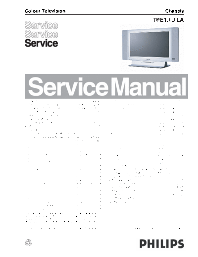
Colour Television                                                                                                                              Chassis
                                                                                                                               TPE1.1U LA


Contents                                     Page                                 Contents                                                            Page
1. Technical Specifications and Connections   2~3                                  PNX2015: DDR Interface                             (Diagram S-B20)42    53~54
2. Safety Instructions, Warnings and Notes    4~ 5                                 PNX2015: Standby&Control                           (Diagram S-B21)43   53~54
3. Directions for User                           6                                 PNX2015: Supply                                    (Diagram S-B22)44   53~54
4. Mechanical Instructions                    7~8                                  VIPER/PNX2015: Display Interface                   (Diagram S-B23)45   53~54
5. Service Modes, Error                                                            VIDEO-DAC                                          (Diagram S-C24)46   53~54
   Codes and Fault Finding                    9~15                                 DC/DC                                              (Diagram S-D25)47   53~54
6. Wiring Diagram                               16                                 SUPPLY+RS232                                       (Diagram S-D26)48    53~54
   Block Diagram                            17~20                                  AUDIO: AMPLIFIER                                   (Diagram S-E27)49   53~54
7. Circuits Diagrams & PWB Layouts                                                 AUDIO: CONNECTORS                                  (Diagram S-E28)50   53~54
   Chassis Overview & Exploded View         21~22                                  ANALOG I/O                                         (Diagram S-F29)51   53~54
                                  Diagram      PWB                                 UART                                               (Diagram S-F30)52   53~54
    Block Diagram                                  (Diagram S-A01)23     53~54     Power Board                                        (Diagram P)55       56~57
    MPIF MAIN: VIDEO SOURCE SELECTION              (Diagram S-A02)24     53~54     SIDE AV Board                                  (Diagram A)58           59~60
    MPIF MAIN: SUPPLY                              (Diagram S-A03)25     53~54     USB Board                                      (Diagram U)61           62~63
    MPIF MAIN: IF+SAW FILTER                       (Diagram S-A04)26     53~54     IR Board                                           (Diagram I)64        65~66
    MPIF MAIN: AUDIO SOURCE SELECTION              (Diagram S-A05)27 53~54         KEY Board                                      (Diagram K)67           68~69
    MPIF MAIN: AUDIO AMPLIFIER                     (Diagram S-A06)28 53~54         DVD Board                                      (Diagram D)70           71~72
    CHANNEL DECODER                                (Diagram S-A07)29     53~54    8. Alignments
    MAIN TUNER                                     (Diagram S-A08)30     53~54       Electrical Instructions&Serial NO.Definition 73~77
    HDMI+SUPPLY                                    (Diagram S-A09) 31 53~54          S oftware Updrade With Portable Memory           78
    I/O+CONTROL                                    (Diagram S-A10)32     53~54       Update DVD firmware for DVD                      79
    VIPER: CONTROL                                 (Diagram S-B11)33     53~54    9. Trouble Shooting                               80~81
    VIPER: MAIN MEMORY                             (Diagram S-B12)34     53~54       Circuit Description                           82~83
    VIPER: A/V+TUNNELBUS                           (Diagram S-B13)35 53~54           IC Data Sheets                               84~94
    VIPER: SUPPLY                                  (Diagram S-B14)36     53~54       Repair Flow Chart                             95~96
    VIPER: EEPROM                                  (Diagram S-B15)37 53~54        10.Spare Parts List                            97~102
    MISCELLANEOUS                                  (Diagram S-B16)38 53~54        11.Different Parts List                            103
    PNX2015: Audio/Video                           (Diagram S-B17)39 53~54        12.Revision List                                   104
    PNX2015: DV I/O Interface                      (Diagram S-B18)40 53~54
    PNX2015: Tunnelbus                             (Diagram S-B19)41 53~54
◦ Jabse Service Manual Search 2026 ◦ Jabse Pravopis ◦ onTap.bg ◦ Other service manual resources online : Fixya ◦ eServiceinfo